Complete Guide to PCBA Testing Process
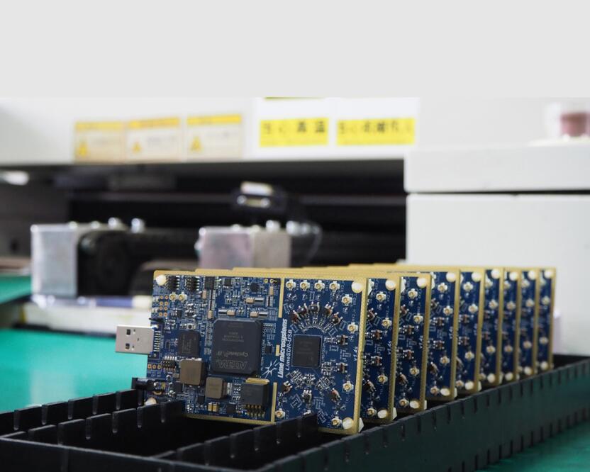
Table of Conent
Table of Conent
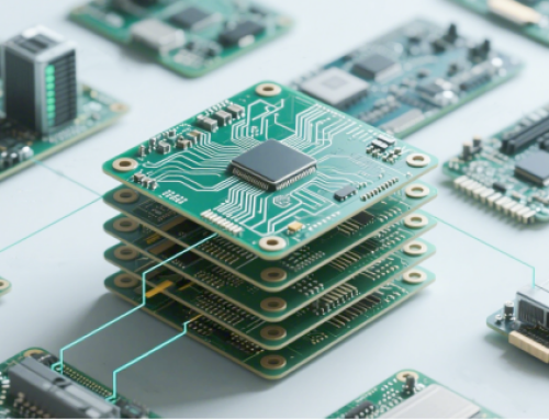
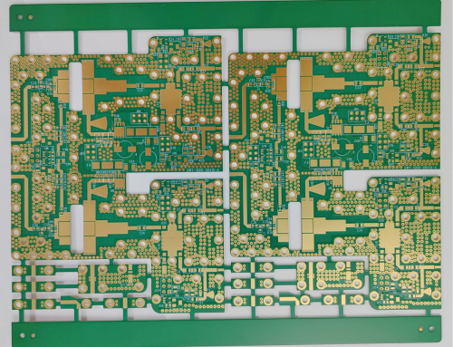
The PCBA (Printed Circuit Board Assembly) testing process encompasses comprehensive quality control from raw materials to finished products, ensuring functionality, reliability, and compliance.
Therefore, it is critical to understand its specific testing process and the problems that may be encountered during the testing process and how to solve them. This article will guide you through the entire testing process.
1. Incoming Quality Control (IQC)
(1)Purpose:
Verify that raw materials (PCB substrates, electronic components, solder, etc.) meet specifications, performance, and reliability requirements.
(2)Inspection Content:
Component appearance (package, silk screen, lead oxidation), dimensions, and polarity;
Electrical parameters (resistance, capacitance, inductance, diode/transistor characteristics);
PCB substrate thickness, pad flatness, via quality, and surface coatings (solder mask, gold plating);
Material certification documents (RoHS compliance, batch consistency reports, OEM test reports).
2. Stencil Inspection
(1)Purpose:
Ensure cleanliness, opening precision, and tension of SMT solder paste stencils meet process requirements.
(2)Inspection Content:
Consistency of stencil opening dimensions with design files (aperture size, shape, positional deviation);
Residual solder paste or contaminants on the stencil surface;
Stencil tension (measured via tensiometer for printing stability).
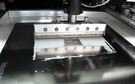
3. Solder Paste Inspection (SPI)
(1)Purpose:
Monitor solder paste printing quality to avoid soldering defects (insufficient solder, excessive solder, misalignment, bridging).
(2)Inspection Content:
Solder paste thickness, volume, position, and shape;
Printing misalignment (alignment relative to PCB pads);
Edge clarity and presence of bridging.
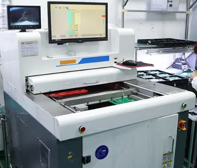
4. In-line Automated Optical Inspection (In-line AOI)

(1)Purpose:
Detect surface mount defects immediately after reflow soldering for real-time process feedback.
(2)Inspection Content:
Missing/misplaced components, polarity reversal, tombstoning, skewing;
Solder joint defects (insufficient/excessive solder, bridging, pad contamination);
Lead deformation or pad damage.
5. SMT First Article Inspection (FAI)
(1)Purpose:
Validate the correctness of the first assembled PCBA before mass production to prevent batch errors.
(2)Inspection Content:
Component designator, type, package, and polarity against BOM;
Placement precision (X/Y offset, rotation angle);
Pad coverage and lead coplanarity (for QFP, BGA, etc.).
6. Reflow Profile Monitoring
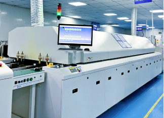
(1)Purpose:
Ensure reflow oven temperature profiles meet requirements for solder paste and components, avoiding soldering defects (cold joints, pad detachment).
(2)Inspection Content:
Heating rate, peak temperature, soak time, and cooling rate compliance;
Temperature uniformity across zones (measured via thermocouple boards).
7. In-Process Quality Control (IPQC)
(1)Purpose:
Real-time sampling inspection of critical processes (e.g., pick-and-place calibration, reflow parameters, manual operations).
(2)Inspection Content:
Batch sampling after first article inspection (hourly/shiftly);
Process parameter compliance (placement pressure, solder paste thickness variation);
Production environment (temperature, humidity, ESD protection).
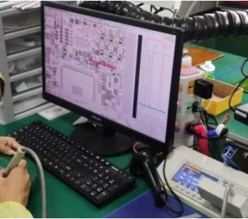
8. In-Circuit Test (ICT)
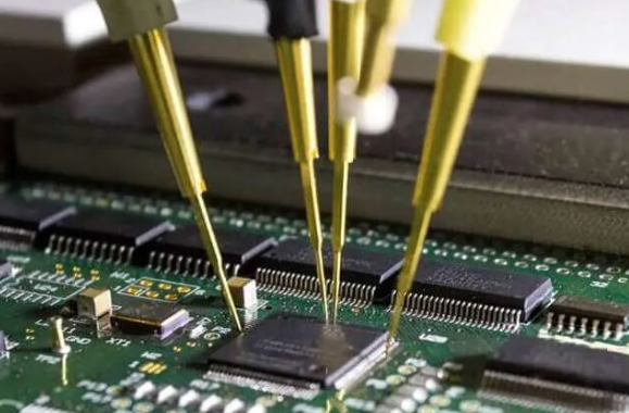
(1)Purpose:
Test circuit connectivity via bed-of-nails or flying probe systems to locate shorts, opens, and component value deviations.
(2)Inspection Content:
Deviation of resistor/capacitor/inductor values from nominal;
Functional pin connectivity of diodes, transistors, and ICs;
Short/opens between circuit networks (e.g., power-to-ground shorts).
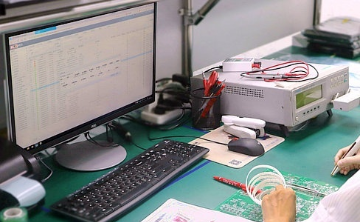
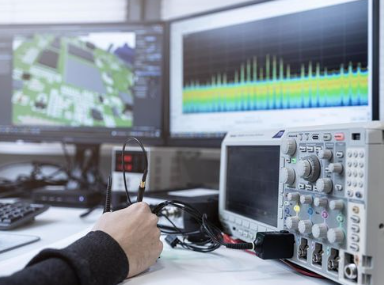
9. Functional Test (FCT)

(1)Purpose:
Validate overall PCBA functionality under power against design specifications.
(2)Inspection Content:
Integrity of input/output signals (voltage, current, frequency, logic levels);
Module functions (communication interfaces, sensor acquisition, drive control);
Human-machine interaction (buttons, displays, indicator lights).
10. Offline Automated Optical Inspection (Offline AOI)

(1)Purpose:
Secondary inspection for complex structures (high density, deep recesses) or sampling, complementing in-line AOI.
(2)Inspection Content:
Same as in-line AOI, focusing on hard-to-reach areas (e.g., BGA peripheral pads, tiny components).
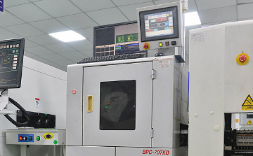
11. X-Ray Inspection
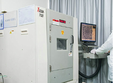
(1)Purpose:
Detect invisible solder joint defects (e.g., BGA, CSP, QFN bottom joints).
(2)Inspection Content:
Solder joint cracks, voids, insufficient/excessive solder;
Solder ball coplanarity and connection integrity;
Alignment between component bottom and PCB pads.
12. Wave Soldering Inspection (Post-Wave)
(1)Application:
For mixed-technology PCBA (SMT + THD), inspect through-hole soldering quality after wave soldering.
(2)Inspection Content:
Via solder penetration (complete filling of through-holes);
Solder joint appearance (saturation, gloss, cold solder, icicles, bridging);
Component damage from heat (e.g., swollen electrolytic capacitors, deformed plastic packages).
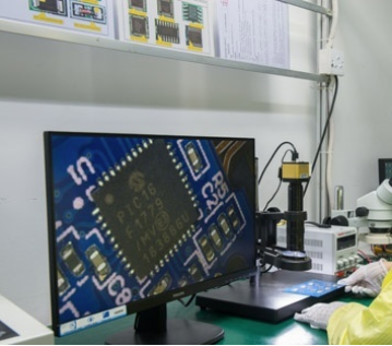
13. Manual Visual Inspection (MVI)
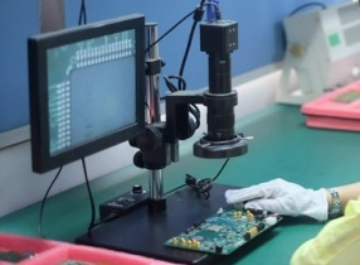
(1)Purpose:
Complement automated inspection for qualitative judgment of complex/irregular defects.
(2)Inspection Content:
Appearance defects (component scratches, PCB substrate damage, blurred silk screen);
Solder joint gloss, wettability, and flux residue;
Connector/cable firmness (mounting stability, contact reliability).
14. Reliability Testing
(1)Purpose:
Validate PCBA performance stability under extreme conditions (critical for military, automotive electronics).
(2)Inspection Content:
Environmental stress tests (high/low-temperature storage, thermal cycling, damp heat, salt fog);
Mechanical stress tests (vibration, shock, drop, bend strength);
Life tests (long-term power-on burn-in, load cycling).
15. Final Quality Control (FQC)

(1)Purpose:
Comprehensive final inspection of completed PCBA to meet customer specifications.
(2)Inspection Content:
Random AOI/X-Ray sampling (ratio based on product class);
Functional retest (complementary to FCT, focusing on customer-specific features);
Labeling and packaging compliance (model, batch number, ESD protection).
16. QA Shipment Inspection
(1)Purpose:
Confirm quality status of PCBA ready for delivery, preventing non-conforming products from reaching customers.
(2)Inspection Content:
Sampling per standards (e.g., MIL-STD-105E) for appearance, function, and packaging;
Verification of shipment documents (test reports, compliance certificates, traceability data);
Simulated transport testing (package compression, shock protection).
17. Possible Problems And Solutions during PCBA Testing
17.1 Incoming Quality Control (IQC)
(1)Common Issues
Component Parameter Mismatch: Resistance/capacitance values exceeding tolerance; IC models inconsistent with BOM.
Appearance Defects: Oxidized component leads, contaminated PCB pads, blurred silk screening.
Certification Gaps: Incomplete RoHS compliance documentation; inconsistent batch test reports.
Polarity/Package Errors: Reversed diode polarity; QFP package dimensions mismatched with PCB pads.
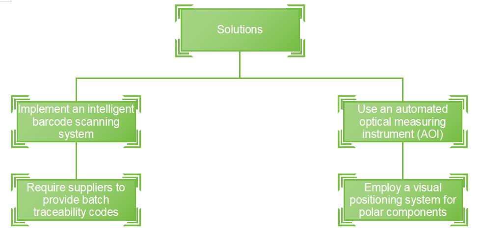
(2)Solutions
Implement an intelligent barcode scanning system to auto-match BOM data with component labels, integrated with a database for RoHS compliance verification.
Use an automated optical measuring instrument (AOI) to check lead coplanarity and pad flatness with ±5μm accuracy.
Require suppliers to provide batch traceability codes, enabling end-to-end traceability via blockchain technology.
Employ a visual positioning system for polar components to auto-identify orientation, achieving a lower misjudgment rate.
17.2 Stencil Inspection
(1)Common Issues
Aperture Size Deviation: Reduced openings for components causing insufficient solder paste.
Tension Degradation: Too many times of use of the stencil causes the tension to be lower than the rated value, compromising printing precision.
Mesh Contamination: Dried residual solder paste clogging apertures, leading to printing leakage.
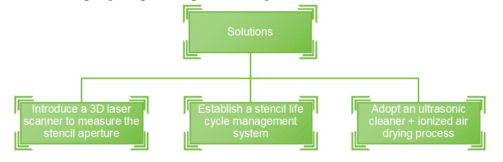
(2)Solutions
Introduce a 3D laser scanner to measure stencil apertures with ±3μm precision.
Establish a stencil lifecycle management system, mandating replacement at <35N/cm tension, equipped with an automatic tension calibrator.
Adopt an ultrasonic cleaner + ionized air drying process, followed by 10x magnifier manual sampling of apertures post-cleaning.
17.3 Solder Paste Inspection (SPI)
(1)Common Issues
Uneven Paste Thickness: Scraper pressure instability causing edge thickness deviation >15%.
Printing Misalignment: Worn PCB locator pins leading to solder paste-pad mispositioning >50μm.
Bridging/Exposed Copper: Solder paste adhesion between fine-pitch (<0.5mm) pads.
(2)Solutions
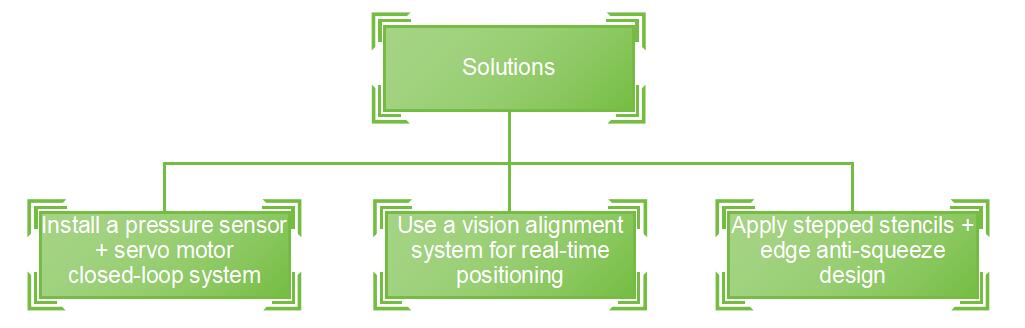
Install a pressure sensor + servo motor closed-loop system to control scraper pressure within ±1% fluctuation.
Use a vision alignment system (±10μm accuracy) for real-time PCB positioning, with automatic mechanical pin compensation.
For <0.3mm pitch components, apply stepped stencils + edge anti-squeeze design, corrected via SPI 3D measurement.
17.4 First Article Inspection (FAI)
(1)Common Issues
Component Misplacement: Capacitor misapplied as resistor; unsynced BOM updates.
Polarity Reversal: Incorrect electrolytic capacitor orientation due to flawed pick-and-place vision lighting.
Coplanarity Failure: QFP lead warpage >0.1mm causing solder joint opens.
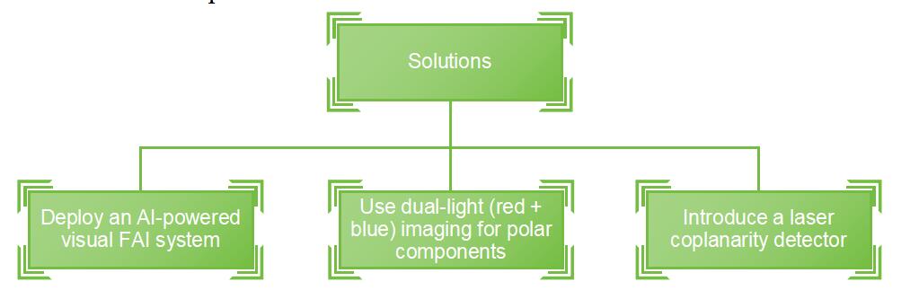
(2)Solutions
Deploy an AI-powered visual FAI system to auto-compare component shape, silk screen, and BOM, with <5-second/component recognition.
Use dual-light (red + blue) imaging for polar components, leveraging machine learning to distinguish polarity marks.
Introduce a laser coplanarity detector for full QFP/SOP lead scanning, triggering automatic line stops for out-of-tolerance results.
17.5 Reflow Profile Monitoring
(1)Common Issues
Abnormal Temperature Curve: Faulty heating zone thermocouple causing peak temperature >250℃ (lead-free solder limit).
Uneven Furnace Temperature: Uneven hot air motor speed leading to intra-board temperature variance >8℃.
Excessive Cooling Rate: Water-cooling leaks causing cooling speed to exceed the specified rate, inducing solder joint cracks.
(2)Solutions
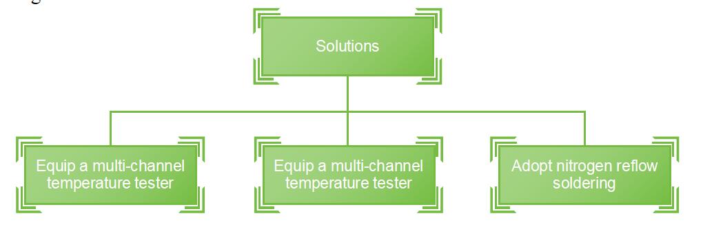
Equip a multi-channel temperature tester (±1℃ accuracy), collecting curves every 2 hours with automatic over-limit alarms.
Regularly calibrate hot air motors (weekly dynamic balance tests) and use a temperature uniformity test board (10-point measurement) in the furnace.
Adopt nitrogen reflow soldering (O₂ <500ppm), adjusting cooling fan speed via PID algorithm for controlled rates.
17.6 In-Line AOI Inspection
(1)Common Issues
High Omission Rate: Invisible bridging on too small solder joints due to low contrast.
High False Alarm Rate: Component color variance triggering increased false positives.
Camera Blind Spots: BGA shadows obscuring adjacent capacitor solder joint detection.
(2)Solutions
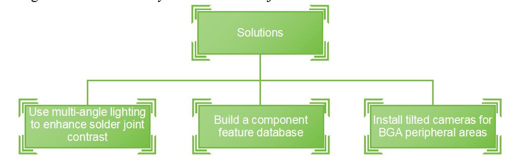
Use multi-angle lighting (0°/45°/90° combination) to enhance solder joint contrast, paired with 3D AOI for height analysis.
Build a component feature database, setting independent detection thresholds for different colors/materials to reduce false alarms to <1%.
Install tilted cameras (15° angle) for BGA peripheral areas, using AI image segmentation to identify occluded solder joints.
17.7 In-Circuit Test (ICT)
(1)Common Issues
Probe Contact Failure: Worn gold-plated probes causing open circuit misjudgment (contact resistance >50mΩ).
Boundary Scan Failure: PCB warpage leading to uneven probe pressure.
Analog Component Misreading: Temperature-affected ESR of electrolytic capacitors causing parameter deviations.
(2)Solutions
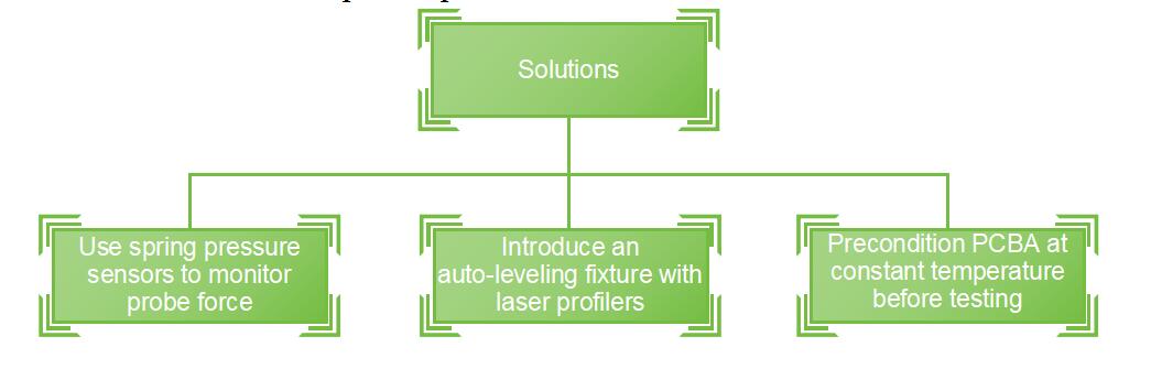
Use spring pressure sensors to monitor probe force (50–100g), replacing worn probes.
Introduce an auto-leveling fixture with laser profilers for real-time PCB warpage compensation.
Precondition PCBA at constant temperature (25℃±2℃) before testing to minimize thermal effects on component parameters.
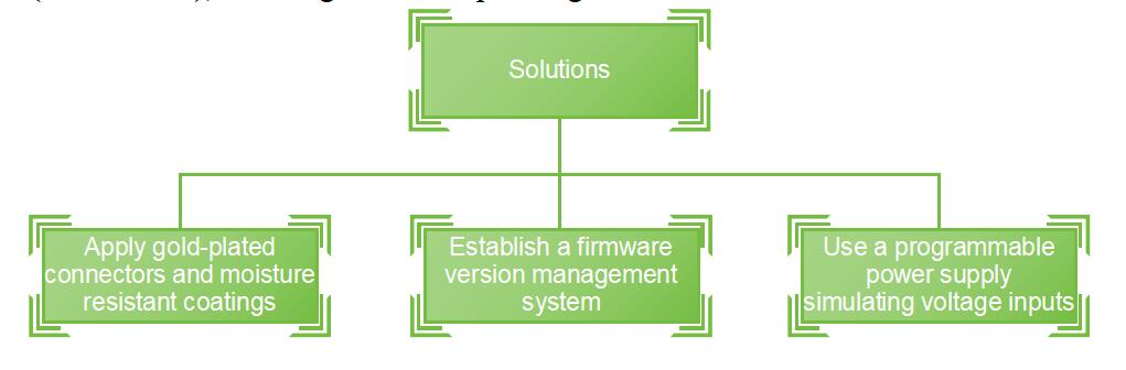
17.8 Functional Test (FCT)
(1)Common Issues
Fixture Malfunction: Oxidized connector pins causing signal interruptions.
Software Incompatibility: Mismatched firmware and test program leading to misjudgment.
Uncovered Edge Cases: Functional failures at input voltages beyond rated ±10% undetected.
(2)Solutions
Apply gold-plated connectors + moisture-resistant coatings, with automatic pin cleaning (contact resistance <10mΩ) before each test.
Establish a firmware version management system to auto-verify PCBA firmware-test program compatibility.
Use a programmable power supply (0.1% accuracy) to simulate wide voltage inputs (rated ±20%), covering extreme operating conditions.
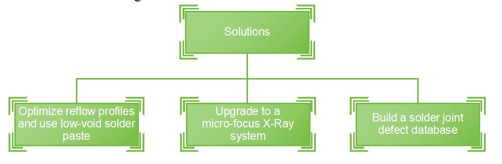
17.9 X-Ray Inspection
(1)Common Issues
Excessive Voids: BGA solder joint voids >20% area compromising reliability.
Layer Separation Omission: Invisible inner-layer delamination missed by low-resolution imaging.
Insufficient Resolution: Blurred details on too small solder joints,hindering joint evaluation.
(2)Solutions
Optimize reflow profiles (extend soak time by 5–10s) and use low-void solder paste (voids <10%).
Upgrade to a micro-focus X-Ray system (5μm resolution), employing computed tomography (CT) for delamination detection.
Build a solder joint defect database, using deep learning to auto-identify internal issues like voids/bridges.
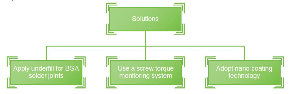
17.10 Reliability Testing
(1)Common Issues
Thermal Cycle Failure: Solder joint cracks after 500 cycles of -40℃~85℃.
Vibration-Induced Shorts: Loose connector contacts causing intermittent shorts.
Salt Fog Corrosion: Inadequate conformal coating (<25μm) leading to pad rust.
(2)Solutions
Apply underfill for BGA solder joints to enhance fatigue resistance.
Use a screw torque monitoring system (±5% accuracy) and pre-vibration connector retention force tests (>5N).
Adopt nano-coating technology (30–50μm thickness) to extend salt fog resistance to 1,000 hours without corrosion.
17.11 Systemic Solutions
(1)Data Closed-Loop Management:
Integrate a Manufacturing Execution System (MES) for real-time inspection data collection, with automatic SPC alarm triggering for anomalies.
Use digital twin technology to simulate inspection processes, predicting equipment failure with >90% accuracy.
(2)Error-Proofing Upgrades:
Deploy RFID chips in pick-and-place machines/test fixtures for automatic material-program matching, achieving 100% error prevention.
Implement a dual-inspection + fingerprint authentication system for critical processes (FAI, QA sampling).
Continuous Improvement System:
Hold monthly PFMEA reviews to address high-frequency defects (e.g., BGA voids, 0201 missing components) with targeted plans.
Build a customer complaint knowledge base, tracing field failures back to inspection gaps for parameter optimization.
18. Summary
PCBA inspection processes span the entire lifecycle from raw material receipt to shipment, combining automated tools (SPI/AOI/X-Ray/ICT/FCT) with manual checks (IPQC/MVI) and routine/reliability testing to intercept defects at every stage. Industries (consumer electronics, industrial control, medical devices) can adjust inspection items and sampling strategies based on product complexity and quality requirements, ensuring high-reliability delivery.
Latest Blog


Contact Info
Phone: +86-755-82882936
Email: [email protected]
WhatsApp: +86-13570802455
Wechat: +86-13570802455
Address: 2nd floor,D Bldg.,Electric Link Technology Bldg.,Gongming,Guangming New Dist.,518106 Shenzhen, China