How to order PCB Assembly Service ?
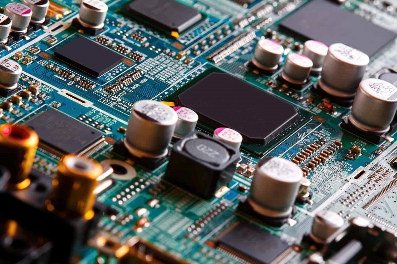
Table of Conent
Table of Conent
The electronics manufacturing industry has undergone significant transformation over the past decade, with the ordering process for Printed Circuit Board Assemblies (PCBAs) evolving into a highly sophisticated and specialized operation. The prevailing trend in modern PCBA procurement is integration and specialization. As the client, your primary responsibility is to provide precise and error-free design data and to select a reliable, communicative assembly partner. This partner will then efficiently manage the integration of the supply chain—including component sourcing and PCB fabrication—along with manufacturing resources, to deliver fully functional, high-quality products.
The complexity of modern electronics demands a meticulous approach to PCBA ordering. Whether you are a startup developing a groundbreaking IoT device or an established company launching a new product line, understanding the intricacies of this process is crucial for success. This comprehensive guide will walk you through each stage of ordering PCBAs, highlighting best practices, potential pitfalls, and strategies for optimizing outcomes.
1 Preparation – Laying the Foundation for Success
The preparation phase is the most critical step in the PCBA ordering process. The adequacy of your preparation directly influences the project’s cost, timeline, and quality. Rushing through this stage or neglecting details can lead to costly delays, redesigns, or even complete project failure.

1.1 Gerber Files
Gerber files are the universal standard for PCB manufacturing. They serve as the “blueprints” of the PCB, containing detailed information for every layer of the board, including the circuit layers, silkscreen, solder mask, drill drawings, and more. Each layer is represented in a separate file, and together, they provide a complete picture of the PCB’s physical and electrical characteristics.
Modern Gerber formats (such as RS-274X) support embedded annotations and metadata, which help manufacturers avoid ambiguities. It is essential to generate these files correctly from your CAD tool, ensuring that they reflect the latest design revisions. Common mistakes include incorrect layer mapping, omitted files, or using outdated versions. Such errors can lead to misaligned layers, missing solder masks, or incorrect drill holes, resulting in non-functional boards.
1.2 BOM (Bill of Materials)
The Bill of Materials is a comprehensive spreadsheet that lists every component required for the PCBA. Each line item should include:
- Reference Designator: The unique identifier for each component on the PCB (e.g., R1, C5, U3).
- Part Number: The manufacturer’s part number (MPN) or distributor’s part number.
- Description: A brief description of the component (e.g., “10kΩ resistor, 1%, 0603”).
- Quantity: The number of units required per board.
- Brand/Manufacturer: The preferred brand or manufacturer for the component.
- Package Type: The physical packaging (e.g., 0603, SOIC-8, BGA-256).
- Value: Electrical values (e.g., resistance, capacitance).
BOM accuracy is non-negotiable. Even a minor error, such as a typo in a part number, can lead to the wrong component being placed—or worse, a component that doesn’t exist. For example, confusing “100nF” with “100pF” could destabilize an entire circuit. It is also important to distinguish between active and passive components, and to note any alternatives or substitutes that are acceptable.
1.3 Pick and Place File
This file provides the automated assembly equipment with the precise locations and orientations of each component on the PCB. It typically includes:
- X and Y Coordinates: The exact center of each component relative to a designated origin point on the board.
- Rotation Angle: The orientation of the component (e.g., 0°, 90°, 180°).
- Side of Board: Whether the component is placed on the top or bottom side.
The Pick and Place file is generated directly from the PCB design software. Inaccuracies in this file can result in misaligned or tombstoned components, leading to soldering defects and board failures.
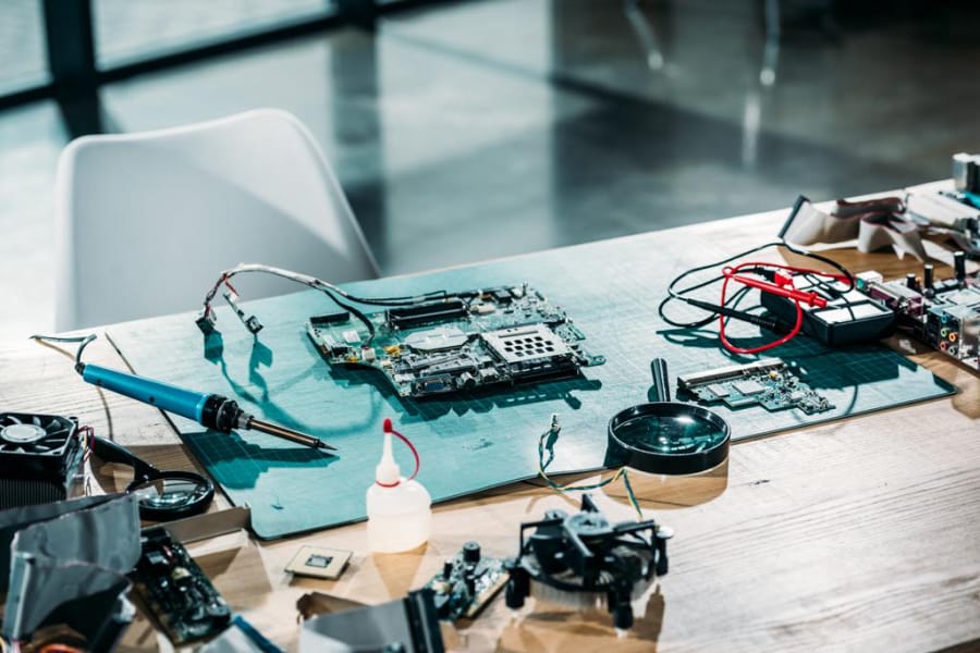
1.4 Assembly Drawing
The assembly drawing is a human-readable document that provides visual and textual instructions for the assembly process. It includes:
- Component Outlines: Diagrams showing the approximate location and shape of each component.
- Polarity Indicators: Clear markings for polarized components (e.g., diodes, electrolytic capacitors).
- Orientation Marks: Indicators for integrated circuits (ICs) and other components with specific orientation requirements.
- Special Instructions: Notes on handling sensitive components, such as RF modules or MEMS sensors.
This drawing is particularly useful for manual assembly or rework processes, and it serves as a reference for quality assurance.
1.5 PCBA Technical Specifications
This document outlines all the process requirements and quality standards for the project. Key considerations include:
- Solder Paste Inspection (SPI): SPI uses optical systems to verify the volume, area, and height of solder paste deposits before component placement. This step is critical for preventing soldering defects like bridging or insufficient solder.
- In-Circuit Test (ICT) or Flying Probe Test: ICT uses a bed-of-nails fixture to test the electrical characteristics of each component and connection on the board. Flying probe tests are more flexible and use movable probes, making them suitable for low-volume or prototype runs.
- X-Ray Inspection: Essential for inspecting hidden solder joints, such as those under Ball Grid Array (BGA) packages or Quad Flat No-lead (QFN) components. X-ray systems can detect voids, misalignments, and insufficient solder.
- Additional Requirements: These may include conformal coating for environmental protection, programming and firmware loading, functional testing, and specific packaging requirements.
Clearly defining these specifications upfront ensures that the manufacturer can allocate the necessary resources and meet your quality expectations.
2 Selection and Quotation – Finding the Right Partner
Choosing the right manufacturing partner is a strategic decision that can make or break your project. The selection process should be thorough and methodical.

Selecting a Manufacturer (PCBA Factory/EMS Provider)
2.1 Capability Assessment
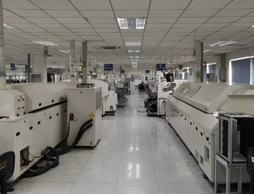
- Equipment: Evaluate the manufacturer’s machinery, including the types of pick-and-place machines (e.g., Fuji, Yamaha), solder paste printers, reflow ovens, and testing equipment. Advanced manufacturers may have automated optical inspection (AOI) systems, X-ray inspectors, and flying probe testers.
- Process Capabilities: Can the manufacturer handle advanced components like BGAs, 01005 chips, or micro-BGAs? Do they have experience with high-density interconnect (HDI) boards, rigid-flex PCBs, or other specialized technologies?
- Quality Control: Look for certifications such as ISO 9001 (quality management), ISO 13485 (medical devices), or IATF 16949 (automotive). These certifications indicate a commitment to standardized processes and continuous improvement.
- Industry Reputation: Check online reviews, ask for case studies, and seek references from past clients. A manufacturer with a strong reputation in your industry is more likely to understand your specific needs and challenges.
2.2 Service Models
- Full Turnkey: In this model, you provide the design files, and the supplier manages everything else: component procurement, PCB fabrication, assembly, testing, and logistics. This is the most hands-off option for the client, but it requires a higher upfront investment. The manufacturer’s supply chain expertise can often lead to cost savings and faster turnaround times.
- Consignment: Here, you procure and supply all the components to the manufacturer, who charges only for the assembly labor. This model gives you full control over component selection and cost, but it also requires you to manage inventory, logistics, and the risk of counterfeit components.
- Partial Turnkey: A hybrid approach where you provide certain critical or long-lead-time components, and the manufacturer procures the rest. This balances cost control with convenience, reducing the administrative burden on your end.
2.3 Formal Quotation (RFQ)
The Request for Quotation (RFQ) process involves sending your complete design package to multiple manufacturers to receive detailed quotes.
- File Submission: Compress all relevant files—Gerber, BOM, Pick and Place, assembly drawings, and technical specifications—into a single archive. Ensure that the files are clearly labeled and organized.
- Clear Requirements: Specify the quantity of boards needed, the desired delivery date, and any special process requirements. Be transparent about your expectations for quality and testing.
- Quote Analysis: The manufacturer’s quote should break down costs into:
PCB Fabrication Cost: Based on the board’s complexity, size, layer count, and material.
Component Cost: The total cost of all components, including any applicable tariffs or shipping fees.
Assembly Cost: Calculated based on the number of components, the type of technology (SMT vs. through-hole), and the volume of boards.
Testing Cost: Charges for ICT, flying probe, functional testing, or other quality checks.
One-Time Costs: Including stencil fabrication, fixture costs for testing, and setup fees.
Logistics: Shipping and handling charges.
Be wary of quotes that are significantly lower than others, as they may indicate compromises in component quality or manufacturing standards.
3 Review and Order Placement – Confirming Details
Once you have received quotes, the next step is to review them carefully and place the order.
3.1 Review the Quotation
Scrutinize each line item in the quote. Pay special attention to:
- Component Pricing: Verify that the manufacturer is using the correct part numbers and brands. Some manufacturers may suggest alternates to reduce cost or mitigate availability issues—ensure these are approved by your engineering team.
- Test Coverage: Confirm that the quoted tests align with your technical specifications. For example, if your board has BGAs, ensure that X-ray inspection is included.
- Payment Terms: Typical terms include a 30–50% advance payment, with the balance due before shipment. Understand the payment schedule and any penalties for delays.
3.2 Sign a Contract/Purchase Order (PO)
The contract or PO should clearly define:
- Price and Payment Terms: The total cost, payment schedule, and currency.
- Delivery Schedule: The agreed-upon timeline for each milestone, from component procurement to final delivery.
- Quality Standards: The acceptance criteria, including allowable defect rates (e.g., based on IPC-A-610 standards).
- Confidentiality: Provisions to protect your intellectual property.
- Liability: Terms for handling delays, defects, or other non-conformities.
Attach the final versions of all technical files to the contract to avoid any misunderstandings.
3.3 Pay Advance Payment
The advance payment allows the manufacturer to secure components and allocate production capacity. Ensure that the payment is made promptly to avoid delays.
4 Execution and Follow-up – Monitoring Production Progress
After placing the order, active management is essential to ensure a smooth production process.
4.1 Component Procurement and Confirmation
In a Full Turnkey model, the manufacturer will procure components on your behalf. Request confirmation of critical components, including part numbers, batch numbers, and certificates of conformity (CoC). This is especially important for components with long lead times or those prone to counterfeiting.
4.2 ngineering Confirmation (EFO)
The manufacturer’s engineering team will perform a Design for Manufacturability (DFM) analysis. They may identify issues such as:
- Insufficient Clearances: Between components, traces, or pads.
- Thermal Imbalances: That could cause soldering defects like tombstoning.
- Pad Design Issues: For example, pads that are too small for reliable soldering.
Respond promptly to these queries to avoid production delays.
4.3 Production and Testing
Request regular updates from the manufacturer, including:
- First Article Inspection (FAI) Reports: Detailed inspections of the first boards off the line.
- In-Process Photos/Videos: Visual evidence of key stages, such as solder paste printing, component placement, and reflow.
- Test Results: Data from ICT, flying probe, or functional tests.
4.4 Logistics and Delivery
Once production is complete, inspect the goods before making the final payment. Verify that the boards meet the agreed-upon quality standards. Then, arrange for shipment using a reliable logistics provider.
5 Summary
- Documents Are Key: The accuracy and completeness of your Gerber files, BOM, and Pick and Place data are the foundation of a successful order.
- Communication Is the Bridge: Maintain open lines of communication with your manufacturer throughout the process, especially during the engineering confirmation phase.
- “You Get What You Pay For”: Extremely low prices may indicate the use of counterfeit components or skipped quality checks. Invest in a reputable partner to ensure reliability.
- Full Turnkey Servicesare recommended for beginners or complex projects, as they reduce administrative burden and mitigate supply chain risks.
By following this structured approach, you can navigate the complexities of PCBA ordering with confidence, ensuring that your project is completed on time, within budget, and to the highest quality standards..
You can also choose a professional and experienced one-stop PCBA supplier: Y&T.
Latest Blog

Contact Info
Phone: +86-755-82882936
Email: [email protected]
WhatsApp: +86-13570802455
Wechat: +86-13570802455
Address: 2nd floor,D Bldg.,Electric Link Technology Bldg.,Gongming,Guangming New Dist.,518106 Shenzhen, China