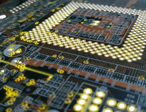
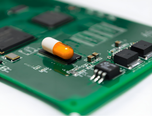
PCB welding mask and silk screen
Table of Conent
Table of Conent
When designing and ordering a printed circuit board, you need to determine if you need to pay extra for welding masks and silkscreen. What is the purpose of these layers? What do they look like?
After reading this article, I hope you will appreciate the benefits of using a welding mask and silkscreen on your PCB, even for prototypes.
Normal Copper
Let’s start with a normal bare circuit board. Select the top copper layer and draw the text, fill, and trace.
Some of the instructions in this article are related to the Copper Connection software. However, the board information and images are relevant regardless of which PCB layout software is used.
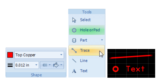
Instructions for the example software. Left: Selecting the top copper layer. Center: Tools for drawing elements. Right: Trace, fill, and text elements drawn on the top copper layer
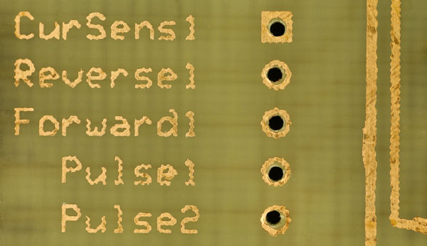
If you were etching a circuit board at home, these elements would look similar to the image below. Notice that the text, fill, and trace are all made of the same material (copper). They all have a reddish-brown metallic color.
Etched Copper PCBs
Clean copper welding is acceptable but will remove copper oxide over time. In this case, you will need to scrub or chemically treat the oxidized copper pads before welding, or the welding will not stick reliably.
Tinning
When you order professionally manufactured circuit boards, they plate the copper with a mixture of tin, lead, silver, and/or other metals. This coating makes it easier to weld, slowing down the oxidation process. The image below shows copper text, traces, and pads plated with a lead-free coating. Notice that the metal is whiter than regular copper.
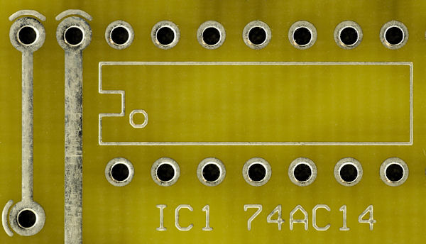
Lead-free plated boards
Tin-plated boards without welding masks or silkscreen are the cheapest. If you want to save money, you can accept it. You don’t need to do anything in your PCB layout software to enable the tin coating, as it is just a basic step in the manufacturing process.
Silkscreen
Unfortunately, when part outlines and text are drawn on the copper layer, they are conductive. You can’t put traces or parts in the same place because the copper text will interfere and change the circuit.
In the layout program, you can place text and part outlines on the silkscreen layer instead of copper. For example, in “Copper Connection”, just select the silkscreen layer before placing text, or select existing text and switch the layer to silkscreen.
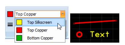
Left: Selecting “Top Silkscreen”. Right: Text on the Silkscreen layer
Copper Connection includes a batch selection feature for your convenience. If you have already made a board with text on the copper layer, you don’t have to move each text element one at a time. Instead, right-click on any copper layer text, choose “Select all text on this layer”, and then select the new layer (top or bottom silkscreen).
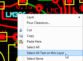
Quickly move the text to the silkscreen layer by choosing “Select all text on this layer”
Now, when you order a board from your favorite manufacturer, be sure to select one of the manufacturing methods that includes silkscreen. For prototype runs, silkscreen is usually limited to the top side of the board, but some manufacturers will offer both sides.
In the photo below, see how the text and part outlines are now a different color compared to the traces and padding. The silkscreen layer is just ink. The ink is non-conductive and can be placed on top of the traces without interfering.
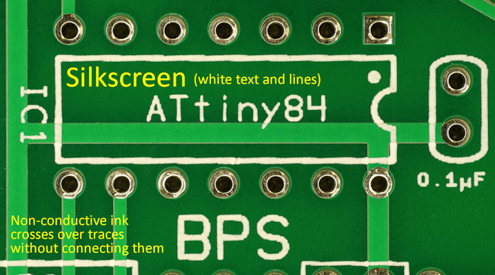
Printed Circuit Board with Tin welding Mask and Silkscreen
In addition to better use of board space, the silkscreen layer is brighter, providing better contrast and allowing for faster hand assembly. The part outline indicates part orientation and makes it clear if you forgot to insert a part. Below are examples of different silkscreen appearances of part outlines produced by different manufacturers.
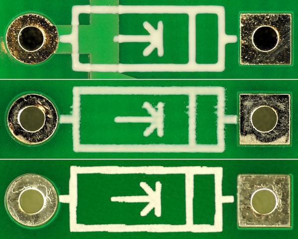
Diode Silk Screen
Welding Mask
When you order silk screen printing, you almost always get a welding mask on both sides. A welding mask (or welding mask) is a coating that protects circuits from corrosion and shorts. It also provides electrical insulation, allowing higher voltage traces to be placed close to each other.
Most importantly, the welding mask keeps welding on pads instead of flowing onto traces, planes, or empty board surfaces. This reduces the likelihood that welding will form bridges (unintentional connections) from one component to another. welding mask is essential for wave welding, which is a mass production technique. However, welding mask also makes hand welding faster, easier, and more accurate.
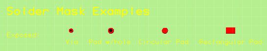
In the photo below, the green coating is a welding mask. See how the welding mask covers the entire board except for the mask. The pads are exposed, allowing you to weld parts to them.
Welding Mask and Welding Mask Bulking
Usually, you don’t have to do anything in your PCB software to enable welding masks. The software automatically punches holes in the mask that correspond to the pads. Additionally, by default, the Copper Connection application enlarges these holes slightly so that moderate manufacturing misalignments (registration errors) do not overlap the pads.

Welding Mask Bulking Amount in the Export Window
Custom welding Mask
In most cases, you won’t be editing or changing the welding mask. You usually won’t even see it in your layout software. If you want, you can view the welding mask in Copper Connect by selecting Layer Color and Visibility in the View menu and checking the box next to the desired welding mask. (Make sure Show Pour and Show Auto Pour are checked in the View menu.)
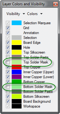
Check one or both layers of the welding mask to see the welding mask
You will see the green mask covering everything except the pads.

Viewing the Welding Mask in a PCB Layout Program
Try placing a rectangle or oval on the top copper layer. Notice that it is covered by the welding mask.
What if you want that rectangle or oval to be an electrical contact, something to weld or connect to a heat sink? The correct approach is to create a rectangular or circular pad of the desired size since these pads are to be exposed.
Alternatively, you can use a regular shape on the copper layer and then add a keep-out area on the welding mask.
1. Select a shape tool (ellipse, rectangle, or polygon)
2. Select the desired welding mask (it must already be visible – see earlier)
3. Select “Keep Fill” (as we want the welding mask to stay out of this area)
4. Draw the shape.
Steps to expose part of the welding mask
This technique is useful for making button contacts (such as keypads). Draw the contact finger with the trace, then cut a space in the welding mask so that the metal on the trace is exposed (not covered by the welding mask).
Button contact with trace exposed through a welding mask
The reverse is also possible. If you want to cover part or all of an exposed pad, such as a via, you can draw the element on the welding mask using Fill (rather than Keep Fill). You will also need to right-click the fill shape and change the Pour Clearance to None (Connect Pour).
Partial welding Mask
Sometimes you need the welding mask to cover part of a pad, rather than exposing the entire pad. An example of this is having a pad under the chip (usually for cooling) that is close enough to other pins that leaving it fully exposed could cause unintended welding bridges.
Start by designing the chip as if it had a smaller inner pad that is only the size of the exposed area. The image below shows the New Land Patten window (in the drop-down menu to the right of the Part tool) with values entered from the Texas Instruments DDA (R-PDSO-G8) PowerPad Plastic Small Outline datasheet. The datasheet calls for a total center pad of 2.94 mm by 4.89 mm, but you only want to enter the smaller exposed size of 2.49 mm by 3 mm.
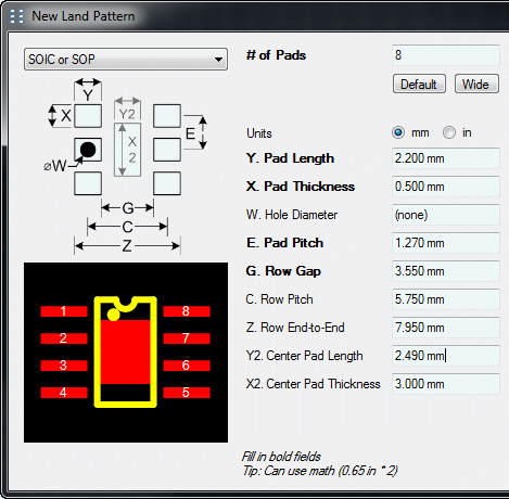
Design the chip using the land pattern window and datasheet
Click the OK button to accept the design, then click on the board to place the part.
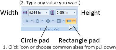
Switch to the Rectangle tool, then select Top Copper Layer and Fill from the Shape section of the ribbon. Roughly draw a rectangle near the PowerPad part, then resize it to the exact size of 2.94mm by 4.89mm by typing those values into the Width and Height in the Size and Position section of the ribbon.

Adding the covered rectangle to the center pad
Select the part and the rectangle select Align Center and then Align Center from the Arrange menu. This will place the rectangle in the middle of the part in the same position as the pad. Don’t worry if the rectangle is above or below the center pad of the part, as the pad always takes precedence over the rectangle. The pad will cut through the welding mask and will accept trace connections even if the rectangle is on top of it.
Officially, the TI part includes a set of six tiny vias in the center. The vias allow heat to be transferred to other layers. I created a version with and without Vias for demonstration purposes.
Below is a view showing the top welding mask (View->Layer Color and Visibility: Check Top welding Mask), all pours displayed (View->Pours->All), and the part sitting on the board. Note that all of the pins and the center pad of the part are exposed, but the larger copper segment in the center is protected by a welding mask.
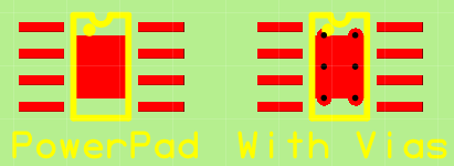
PowerPad Welding Mask
Parts with vias will have some extra welding traces around the edges, but may still be acceptable. However, be aware that the welding mask will expand (get larger) to compensate for misalignment during manufacturing. If the mask expands enough to hit the outer pins again, you can save yourself all the hard work. If this happens, you can make the center pad smaller.
Enable X-ray Vision (View->X-Ray Vision->All) to see the larger copper rectangle around the pads.
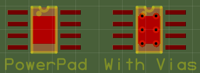
PowerPad welding Mask with X-Ray
Combining pure copper shapes (circles, arcs, lines, rectangles, or polygons) with pads is a great way to create virtual pads that are only partially exposed through the welding mask.
Tented Vias
A via is a hole that connects one layer to another but is not intended for any part to be inserted into. Often you want to expose a Via so you can test the board, or if you make a mistake on the board, you have an optional place to insert a wire or hole. This is the default setting.
If you are sure your board is perfect, and your fabrication/welding methods allow for vias, then you can use a welding mask and silkscreen in all vias. This prevents corrosion and accidental shorts and provides more surface area for text and part outlines.
In Copper Connections, you can select Tented Vias in Board Properties in the File menu. Note that this window controls other layers, such as silkscreen and welding mask, as well.
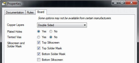
Board Properties Control Silkscreen welding Mask and Tented Vias
After clicking OK, the results will be reflected on the screen. If you choose tented vias, you can still manually edit the welding mask and adjust the text position to expose specific vias if needed.
Prototype Selection
When I first started making printed circuit boards, I chose two-layer boards without welding masks or silkscreen because of lower costs. This forced me to place part labels on the copper layer or abandon labels without enough space.
As the volume grew, I realized that this was a false saving. It takes a lot of time to figure out the location of parts on a board that lacks adequate labels, especially if the board was designed a while ago. Lack of labels can cause parts to be welded in the wrong place or forgotten completely.
Shenzhen Assypcb SMT: Lack of welding mask is not a big problem, but welding mask can reduce welding time by guiding welding to the pads. (I have never encountered a manufacturer who provides silkscreen without welding mask anyway.)
Latest Blog

Contact Info
Phone: +86-755-82882936
Email: [email protected]
WhatsApp: +86-13570802455
Wechat: +86-13570802455
Address: 2nd floor,D Bldg.,Electric Link Technology Bldg.,Gongming,Guangming New Dist.,518106 Shenzhen, China