A Guide to PCB Assembly Problems And Solutions
Table of Conent
Table of Conent
We are surrounded by the technology. Technology is all around us, whether at home, at work, or in our leisure time. It is important to ensure that the PCB Assembly Process meets standards.
PCB assembly is not without its challenges. This blog will help you to navigate common problems. These problems occur during PCB assembly. This blog also offers practical solutions to ensure your assemblies are efficient and reliable.
To begin troubleshooting an electronic circuit board, you must first determine if it is faulty and what problems it has. PCB Assembly failure causes can range from minor issues to major ones. PCB defects can be classified into four main categories.
- Physical Damages:PCBs can be damaged by water, dust, heat, oxidation,or vibration. Physical damage is often indicated by obvious signs such as corrosion.
- Design Flaws:Human errors can also lead to PCB design faults. Incorrect component placement and improper material selection are examples of actions that can lead to a reduction in performance efficiency.
- Failures of components:PCBs, like most devices, rely on many electronic components. These wear out over time. Components can malfunction or stop functioning as they age. It’s important to know which parts are more likely to fail than others.
- Manufacturing Errors:Small oversights can have a significant impact on PCB functionality. Sometimes manufacturers are able to catch these issues late in the manufacturing process. Other times, an operator may not be able to see a problem until it is used.
The list above is not complete, as there are many other problems that may occur. Below are some common PCB issues and signs.
PCB Assembly Failure
1.Design Issues
1.1 Poor Thermal Control
PCB assemblies produce heat during operation. Thermal management can be inadequate. It results in overheating and damage to sensitive components.
Solution:
Designers can address this by integrating heat sinks or thermal vias into the design.
They can select materials that have high thermal conductivity. This can also help efficiently disperse heat and maintain optimal temperatures.
1.2 Footprint Mismatch
The size of the SMD components or the pin spacing does not match Gerber/BOM.
Solution:
Check the footprints of the components against the Bill of Materials before finalizing your design. Use design rule check (DRC) tools.
Mismatches with regard to pin orientation or package size, pad spacing, and pad spacing should be flagged. Validate footprints by conducting a DFM with the assembly team.
1.3 Design Flaws in Pad/Hole Designs
The mechanical strength and solder adhesion of the solder is not adequate.
Incorrect hole diameter: Poor fit of the lead (too tight/loose), resulting in solder voids and pull-out.
Uneven Pad Layout: Asymmetrical heat dissipation causing soldering inconsistencies.
Solution:
Place vias away from BGA, QFN, or fine-pitch parts. They increase the risk of shorts and complicate rework. If necessary, use blind/buried vias to cover internal layers.
Based on the component datasheets, IPC-2221 guidelines, and solder pad measurements (length, width, and thickness), base your dimensions of solder pads. Minimum annular rings should be based on board tolerance and thickness.
design flow in pad design
2.Component Issues
2.1 Counterfeit Parts
Components may be substandard or counterfeit. They are usually detected using XRF material analyses or chip photography.
Solution:
We must work with reliable suppliers. Y&T Technology guarantees that all of its components are genuine.
2.2 Polarity/Orientation Errors
The polarity of electrolytic capacitors is not marked. Diodes have reverse polarity marked on them. The pin alignment of ICs is incorrect. This can cause functional failures following soldering.
Solution:
It is important to replace and remove these defective components as soon as possible to prevent future functional failures.
2.3 Physical Injury
Damaged components are caused by improper handling or transport. Cracks, bent pins, or missing pads are all examples of this.
Solution:
Avoid collisions by packaging components properly during transport.
2.4 Oxidation/Corrosion
Leads can lose their shine or become soaked, which causes contamination of the surface. Solderability is affected.
Solution:
Use protective coatings to prevent moisture and contaminants from reaching the lead.
2.5 Component Floating/Tilting
The inserting is not secure. The soldering is not done with enough holding force. The wave may be too buoyant. These can cause misaligned parts, incorrect lead immersion, and failed soldering joints.
Solution:
Do an excellent job in training employees to ensure correct operation.
Maintained regular inspections and commissioning to ensure that machines are operating correctly.
2.6 Component Missing/Excessive Placement
Errors in the programming and feeding of the feeder can result in missing components or duplication. Functional failures and shorts can result from this.
Solution:
Check the first board manually or automatically.
Verify all components are correctly positioned and present. Catch any misalignments of the feeder early.
Replace worn parts immediately after routine inspections. Feeders should be calibrated to disperse components at exact angles and intervals.
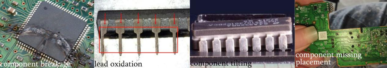
Component Issues of component breakage,led oxidation corrosion component tilting,component missing excessive placement
2.7 Material Composition Errors
The substrate is not compliant with the standard or the plating is wrong.
Solution:
Use only certified substrates, and use the correct plating technique.
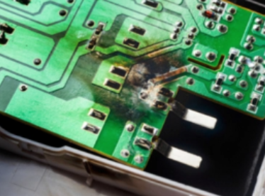
3.Environmental Issues
3.1 Humidity and Moisture
The humidity is too high. Or the PCB storage isn’t protected well. This can cause flux failure or pad/pin oxidation. This also leads to poor wetting, increased voiding, or flux splashing when soldering. QFN and BGA parts are not dry-packed properly. Moisture absorption can lead to delamination during reflow-soldering.
Solution:
Moisture barrier bags (MBBs) are the best way to store PCBs and other components. Desiccant packs (HICs), humidity indicator cards (HICs), and seal bags should be available.
For MSCs that are awaiting assembly, use dry cabinets or climate-controlled vaults. If the floor life is exceeded, bake components according to JEDEC JSTD-033. Components can be stored in aluminum laminate bags with heat-sealed edges.
Use UV-curable silicone or acrylic coatings to prevent moisture from entering the assembly after it has been completed.
3.2 Cleaning Agent Residue
Ionic contamination exceeds the IPC-5701 limit.
Solution:
You can choose different cleaning agents depending on the type of contamination. Source cleaners comply with IPC-CC-830 (solvent cleaning) or IPC-8010 (aqueous cleansing). Automated optical inspection (AOI), to map the flux distribution after reflow. For extended cleaning, flag boards with excessive bridging and non-uniform coverage of flux.
3.3 Adhesive failure
Low bond strength post-cure or Tg below standard.
Solution:
Select adhesives with Tg >=20degC over the maximum operating temperature. Removing oils, oxides, and mold release agents. Surfaces need to be cleaned and roughened for adhesives to adhere properly. Low Tg and bond strength can be caused by an insufficient curing temperature or time. Track cumulative exposure to cure using time-temperature integrators (TTIs).
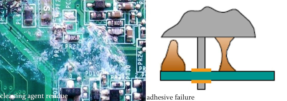
Environmental Issues of cleaning agent residue,adhesive failure
4.Functional Issues
4.1 Parameter Deviation
Instability performance or values that are out of tolerance.
Solution:
Components should be purchased from distributors who are certified to ISO-9001. Perform a 100% automated optical inspection of passive components to check for physical damage.
4.2 Short/Open Circuits
Contact resistance is poor or there are intermittent failures of connectors.
Solution:
Use pad spacing that is compliant with IPC-7351. To minimize shorts due to misaligned reflow, avoid placing vias underneath BGA pads.
No-clean fluxes with low ionic residuals will prevent dendritic formation over time. A low-temperature solder is recommended to prevent overheating and openings.
short open
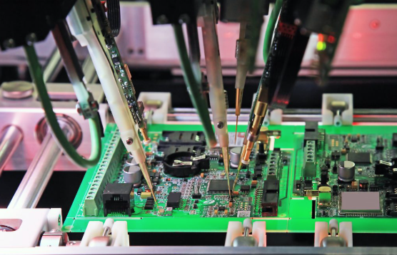
5.Soldering Process Issues
5.1 Voiding at BGA/CSP Joints
Microvias can trap moisture or flux gases.
The PCB manufacturing process is not good for hole filling.
Solutions:
Vacuum reflow ovens can be used to reduce voids.
You can also require X-ray inspections per IPC-7095 to ensure 100% BGA coverage.
5.2 Solder balling
Moisture in solder paste or PCB substrate vaporizes during reflow.
Splatter is caused by excessive solder paste or temperature spikes.
Solutions:
If the humidity level is above a certain threshold, bake PCBs before assembly.
Add solder masks between pads to contain the paste. Solder paste is prevented from settling on the pads.
5.3 Cold Solder Joints
The pads are contaminated if they have not been heated enough during the reflow.
Lead oxidation in the component can cause wetting to be impaired.
Solutions:
To ensure melting, extend the soak zone duration on the reflow profile.
Before assembly, clean pads with plasma to remove oxides.
5.4 Component Lifting (Tombstoning)
Asymmetric thermal mass can cause uneven pad heating.
The volume of solder paste is not balanced or the component placement is misaligned.
Solutions:
Use symmetrical layouts of thermal reliefs and pads.
To improve wetting, choose a high-activity paste (e.g. SAC305).
5.5 Solder Bridge
Stencil misalignment or oversized apertures deposit excess paste.
Low-viscosity solder paste spreads during reflow.
Solutions:
Use SPI (Solder paste inspection) to flag any deviations in the volume of the solder paste.
Angle the wave soldering conveyor for optimal separation.
5.6 Incorrect Component Orientation/Position
Human error appears during insertion. Misaligned jigs or unclear assembly drawings. This will result in misplaced solder and leads.
Solution:
Strengthen the employee training for standard operations.
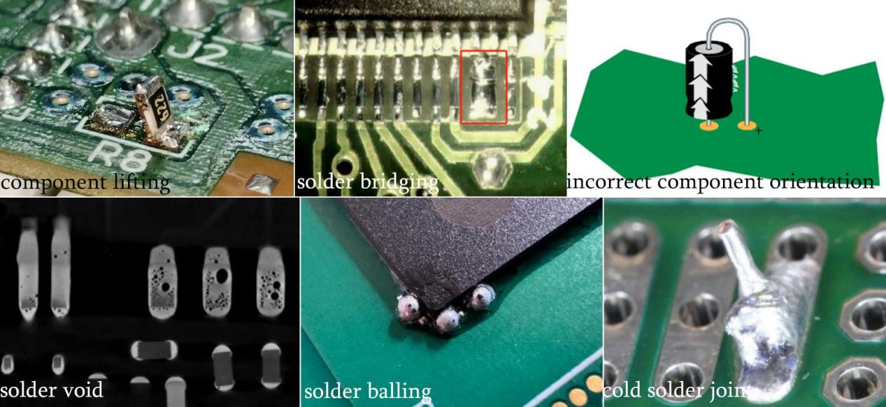
Soldering Process Issues of Soldering Process Issues of component lifting,solder,solder bridging,incorrect component orientation,solder void,solder balling,colder join
5.7 Wave soldering defects (Blowholes and Icicles)
If moisture is found in the through-holes, or on the conveyor angle, this is not correct.
Solutions:
You can bake PCBs in advance to remove moisture.
You can also optimize the wave nozzle pressure as well as flux spray uniformity.
5.8 Uneven Solder Joints
Reduced solder fluidity due to oxidized or uncleaned tip. Rapid air movement or premature flux volatilization can lead to irregular solder joints. Stress fractures are more likely to occur when mechanical strength is insufficient. Sharp spikes can cause high-voltage short circuits or arcing.
Solution:
Clean and rinse the iron tips regularly. Replace them as soon as they wear out. Select the correct flux. Limit the soldering time for each joint to maintain flux activity. Improve your soldering technique and make sure you use the right-hand placement and motion. Avoid spattering and voids by using high-quality paste.
5.9 Pad Leaning/Tilting
A lack of vacuum pressure may cause components to lift off the PCB surface. Partially contacting the pad results in a semi-wetted joint with reduced vibration resistance. Over time, this is susceptible to fatigue cracking.
Solution:
Optimize vacuum pressure in placement equipment. Make sure it is sufficient to securely hold the component. Flatten PCBs that are warped using vacuum chucks or thermal reconditioning.
Check component coplanarity. Reject bent bodies or bent leads from suppliers. Staff should be trained on vacuum troubleshooting and tilt signs, as well as nozzle selection. Implement an In-Process inspection in order to detect drift as early as possible.
5.10 Mechanical stress
Over-spray pressure can displace components. An incorrect ultrasonic frequency can damage electrolytic capacitors. QFP lead can be deformed due to cleaning fluid impact. Vibration stress causes micro-cracks to appear on BGA balls.
Solution:
Avoid component displacement by controlling spray pressure. Electrolytic capacitors should not be subjected to ultrasonic damage.
Avoid QFP lead deformation due to fluid impact.
Avoid rough handling and use vibration-dampening devices to reduce vibration-induced BGA cracking.
5.11 Lead deformation/breakage
The force of insertion is excessive. Lead forming is not done properly. The wave impact may have caused mechanical stress. These can result in damaged leads, circuits that are open, or difficulties with subsequent rework.
Solution:
Use precision automated machines equipped with force sensors that control the insertion force.
Enforce gentle handling for manual insertion. Avoid direct pressure on leads by using vacuum pick-up tools or tweezers.
Use pins or clamps to fix the PCB. Align the leads parallel to wave flow to reduce lateral stress.
5.12 Head-in-Pillow (HIP)
BGA ball/pads oxidize or PCB warpages occur during reflow.
The temperature is insufficient to melt the solder spheres.
Solutions:
Store BGAs in moisture-proof bags and bake them before storing.
5.13 Component Corrosion
Acidic cleaners may erode metallic coatings. Alkaline cleaners discolor pure tin/silver immersion coatings. Corrosion of connector pins increases contact resistance. It can cause signal transmission problems. This is because the corrosion of nickel pads can reduce the adhesion between soldering joints. Cold solder is the result.
Solution:
Use specialized electronic cleaners or pH-neutral electronic cleaners. Avoid contacting metallic coatings. Validate the cleaning agents with respect to specific surfaces. This will prevent corrosion and ensure reliability.
Soldering Process Issues of mechanical stress,Head-in-Pillow,lead deformation,Component Corrosion
6.Testing Issues
6.1 Functional Test Failure
Insufficient scope of testing is a common problem in PCB testing. Test procedures may be neglected or rushed. This can lead to errors that are not detected until the end of production. Incorrect consideration of product-specific test environments can compromise PCB performance. Humidity levels, temperature fluctuations, and mechanical vibrations are all environmental factors. These factors directly affect product quality and the ability of the product to withstand actual conditions.
Solution:
Circuit board testing is used by PCB manufacturers to verify that the assembly process has been completed. It ensures that each component pin is properly connected to its respective circuit net. Test points need to be strategically placed in order to conduct comprehensive tests. Design for Test (DFT), guidelines should be followed. Manual validation is necessary if test points are not covered.
6.2 Flying Probe Testing
The oxidation of the probes increases contact resistance and opens are more susceptible to misjudging.
Solution:
Pay attention to routine inspections and replace the oxidation sensor in time.
6.3 ICT (In-Circuit Test)
The bed of nails is not accurate. Short circuits can occur. The spring pins become less effective as they age. This causes a contact that is unstable and inconsistent.
Solution:
Replace the spring pins and debug the fixture’s accuracy.
testing failure
7.Packaging Issues
7.1 Damaged Rays/Reels
The reels and trays have been damaged. This is not good for transmission.
Solution:
During transit, use ESD-safe plastic trays with foam inserts. Robotic arms equipped with vacuum grippers can be used to load and unload reels. This reduces manual handling errors.
7.2 False packaging
Packaging that is anti-ESD is not appropriate for sensitive electronics.
Solution:
Direct contact between components and non-ESD material is prohibited. Bags should be heat-sealed using conductive tape, not plastic clips, to create the Faraday cage. Add humidity indicator cards for devices that are sensitive to moisture.
8.Summary
Understanding the issues that PCBs face and how to avoid them is crucial for smooth operation. To avoid problems from happening, effective printed circuit board troubleshooting involves working with a PCB manufacturer who is qualified and experienced.
Y&T Technology has a team of knowledgeable, dedicated professionals you need to identify PCB problems and make any necessary alterations. We can provide you with any kind of PCB assistance you require.
Y&T Technology’s award-winning customer service team is available to answer any questions.
Latest Blog

Contact Info
Phone: +86-755-82882936
Email: [email protected]
WhatsApp: +86-13570802455
Wechat: +86-13570802455
Address: 2nd floor,D Bldg.,Electric Link Technology Bldg.,Gongming,Guangming New Dist.,518106 Shenzhen, China