A Step-by-Step Guide to Assemble a PCB
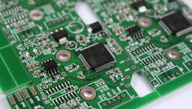
Table of Conent
Table of Conent
Electronic products have become a part of modern life. PCBs are one of the most important components. Have you ever made your own electronic devices by hand when you look at these intelligent products? It is easy to make a mistake without a tutorial.
This article provides a comprehensive guide on manual PCB Assembly. This article covers the preparation, assembly, testing, and debugging. It can be used for small-batch prototypes as well. These 5 core steps will increase your success rate by 95%.
1.What is PCB Assembly?
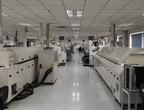
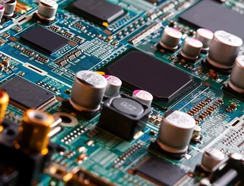
The PCB assembly process involves mounting components on the circuit board to ensure they work in a specific way. PCBAs can be used in more complex applications or to build electronics with a specific purpose. PCB assembly is either automated or manually done, but automated assembly has become more common in recent years thanks to advances in robotics. There are some steps that are usually manual, depending on the type of PCB being made.
2.Pre-assembly Preparation
2.1 Preparation of Tools and Materials
(1)Tools Required
Soldering iron (fine tip for SMT and thicker tip through-hole).
Solder (rosin core).
Flux (enhances solder flow).
Tweezers (for handling SMT components).
Diagonal cutters (for trimming lead).
Desoldering the wick/pump (for rework).
Multimeter (for continuity and resistance tests).
PCB clamp/holder (to secure board during assembly).
Anti-static wristband (to prevent ESD damage).
Magnifying Glasses or Microscopes (for small SMT components, optional).
tools preparation
(2)Materials
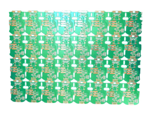
Blank PCB with copper traces (and pre-drilled holes).
Electronic components (resistors and capacitors, ICs and connectors, etc. sorted according to type and price).
Solder paste (for SMT parts, if reflow soldering is used).
Cotton swabs and isopropyl Alcohol (for cleaning flux residue).
2.2 PCB Layout and Preparation
(1)Preparation of PCB
Inspect PCB: Check the board for defects.
Test the electrical continuity: Using the multimeter, check the continuity.
Insulation test: Measure the resistance between adjacent signal traces.
(2)Cleaning PCB
Contamination removal: Use IPA for oil/fingerprints. Use a neutral detergent to ultrasonic-clean old flux residue.
Pad pre-treatment: Remove the oxidation from the solder mask and protect it.
(3)Positioning and Marking Aid
- Fiducial marking
Optical fiducials for SMT: Add 3 copper marks to PCB edges as pick-and-place machine alignment.
Manual alignment: Draw crosshairs on PCB corners using a marker. Align it with the grid paper on your workbench to ensure uniform component orientation.
Fiducial marking
- Special Area Preparation
BGA pads: Inspect the pad’s flatness with a magnifying glass; reject boards that have a large depression in order to prevent solder bridges.
Oxidized pad: Sand and activate using flux via soldering Iron.
Damaged pads (copper losses 30%): Connect vias adjacent to jumper wires to ensure electrical continuity.
Through-Holes Deburr clogged throughs with a reamer for smooth lead insertion.
Hole Diameter: Match the hole diameter to that of the lead (too large can cause wobbling, and too small will result in insertion force problems).
- For SMT
To remove fingerprints and oil stains, use a cotton swab dipped into isopropyl ethanol (IPA) to clean the pads.
If the pads are gray, activate with flux (to improve solder wettability)
(4)Component Layout
- Scheme and Layout Review:
Verify that the component footprints and schematics match. Verify that there are no redundant footprints or missing test points. Verify component placement, polarities, orientations (diodes and capacitors), and orientations.
- Component Preprocessing:
THT Components:
Use sandpaper to remove lead oxide or a wire brush.
Bend leads to align them with PCBs (adjust spacing if necessary with pliers).
- SMT Components:
Check the terminals on components with a magnifying lens (if they are oxidized, use absolute ethanol to clean them);
Handle with tweezers and avoid touching the pads.
Avoid ESD damage by using an anti-static belt when handling sensitive components.
Confirm the coplanarity (correct with a leveling device to avoid cold joints if necessary) of the leads for QFP/SOP packaged ICs.
3. Surface-Mount Technology(SMT) Assembly
Surface-Mount Technology (SMT) Assembly
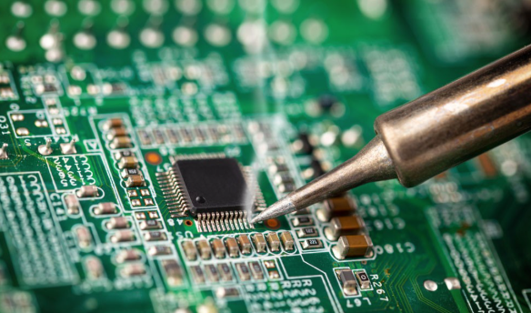
3.1 Hand Soldering (for Small Quantities)
(1)Apply flux: Dab on a small amount if you are using flux-cored solder. This helps to wet the pads.
(2)Place components: Use the tweezer to align pins on pads.
(3)Tack Solder One Pin: Secure your component by first soldering a corner pin, and then check alignment. Adjust if necessary.
(4)Solder the remaining pins: For SOIC/QFP ICs, drag the iron tip gently along the pins and feed the solder when necessary. Solder one pad and place the 0603/0805 component. Then solder the second pad.
3.2 Solder paste + Reflow (for large batches)
(1)Apply solder paste: Use stencils and squeegees to deposit the paste on pads.
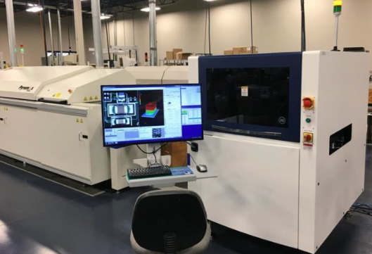
(2)Solder paste inspection: Solder paste inspection machines (SPI) are used to inspect the paste after it has been applied. SPl devices are available in two different types: 2D and 3D.
The height and width can be measured by 2D equipment. 3D machines calculate the volume, length, and width of the solder paste. These devices can also detect errors in assembly, such as missing solder and paste.
(3)Component Placement: Use a pick-and-place tool or tweezers for positioning components on the paste.
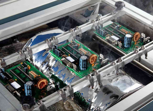
(4)Reflow: Heat up the board with a reflow station or a hot-air station, according to the temperature profile of the paste you are using.
3.3 Automated optic inspection (AOl).
The AOl system uses optical devices to inspect solder joints on PCBs and component orientation. The systems identify defects such as missing parts, soldering difficulties, misalignments, incorrect component orientations, lifted and misplaced elements, open circuits and solder shorts, and excess or insufficient solder. This helps in quality assurance.
Automated optic inspection
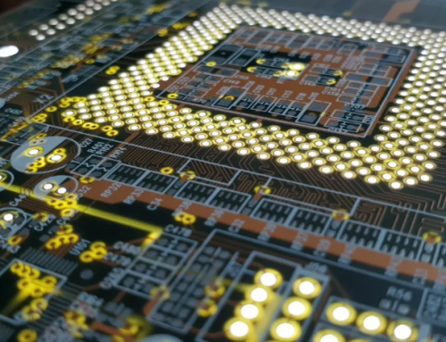
3.4 X-ray examination
The X-ray method is a form of non-destructive (NDT) testing that uses X-rays in order to produce images of internal structures. This method is for complex multilayer circuit boards that have fine-pitch components. It reveals any faults in the solder joints on the board.
3.5 Flying probe tests (FPTs)
The FPT method is an automated way to test PCBs. It detects open circuits, shorts, and other component attributes like resistance, capacitance, and inductance. The testers are made up of multiple movable probes that can be moved freely in XYZ directions.
The probe is highly adaptable and flexible for small production runs and frequent design modifications.
During the testing phase, the flying probe tester is programmed with netlist data taken from the design file.
The tester moves the probes around the PCB to measure electrical properties such as resistance and capacitance.
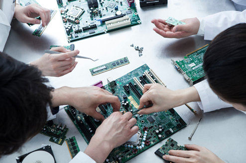
4. Assembly of Through-Hole Components
4.1 Components Inserting
(1)Install Short/Low Components First: Install smaller components (resistors and small capacitors) first to avoid blocking adjacent pads.
(2)Align Pins With Pads: Push the component leads through PCB holes on the top side (component side), making sure they protrude a little bit on the solder side.
(3)Secure components: For tall parts (connectors and transformers), clamp them or temporarily hold them.
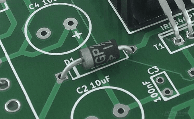
(4)Orientation alignment: Ensure that components are installed in the correct orientation (reverse installation can burn components).
4.2 Soldering
Soldering
(1)Pre-heat pad: Use the iron tip to contact the pad and the lead at a 45-degree angle. The pad will darken slightly.
(2)Apply Solder: Feed the solder into the joint, not the iron. Continue until a small fillet appears. Avoid over-soldering.
(3)Remove iron: Allow 1 sec for the soldering to solidify, before removing the board.
4.3 Leads Trimming
Trim excess leads with pliers that have a flush-cutting blade. (Leave about 1mm to prevent pad lift).
ESD Control: Clean the trimmings with a sticky pad or compressed air immediately to avoid metallic debris shorting.
5.Inspection and Rework
5.1 Inspection
(1)Visual Inspection
| Inspection Item | Acceptance Criteria | Common Defects & Identification |
| Solder Joint | No burrs, no bridging. | Cold joints (dull granular surface), solder bridge (pads adjacent connected), insufficient solder |
| Component | Correct polarity; no Distance is a factor that can be used to determine whether or not a person is displaced. |
Missing parts, misaligned ICs (reversed polarity), mismatched BOM lists (missing components) |
| Pads and Traces | No pad delamination; no trace shorts/opens | Damaged pads (copper losses >30%) and trace spacing 0.1mm. |
| Flux Residue | There are no obvious white/yellow stains around joints | Excessive sticky residue (potential conductive corrosion) |
(2)Continuity test: Use the multimeter to check for connections between component leads and pads (ensure there are no shorts or opens).
5.2 Rework
(1)Component Replacement:
- Components with Through-Hole: Use a desoldering wick or a desoldering wick to remove the old solder. Pull out the component gently while heating the joints.
- SMD components: Apply heat to the component with a reworkstation. Once the solder has liquefied, lift the component usinga tweezer. Apply the paste to the pads and then solder the part.
(2)Pad Delamination/Damage:
- Mild damage (Copper loss 50%): Cleanthe area, apply thin flux, and bridge with enameled wire to an adjacent pad/net (secured with high-temperature taping to prevent stress fracture).
- Complete pad loss: Identify the inner-layer trace (via) by soldering directly to the exposed copper.
(3)THT Cold joints/Bridgings:
- Solder Bridge (Short Circuits): Apply flux to the bridged areas.
Heat the iron and place the solder wick on the bridge until the excess solder has been absorbed.
- Cold Solder Joints: Add flux to the joint. Reflow the solder with the soldering tool until it flows smoothly.
(4)SMT Misalignment/Bridging:
- Misalignment of Components (Terminals not fully on Pads): Heat component witha hot air station, until solder melts. Realign with tweezer.
- QFP Bridging: Use an ultra-fine tip iron with minimal solder to swipe along the lead gaps and separate joints using surface tension. To do extensive bridging with solder, first remove the excess solder using a wick. Then re-solder every lead.
QFP Bridging
5.3 Post-Rework Processing
(1)Residue cleaning: Wipe the reworked area with isopropyl ethanol to remove flux, and metallic debris and prevent long-term corrosion.
(2)Secondary inspection: Recheck repaired joint visually and continuity; retest IC functionality.
6.Cleaning, Testing, And Final Debugging
6.1 Cleaning
(1)Purpose of Cleaning:
To prevent:
Corrosion or dendritic growth;
Signal interference;
Poor adhesion of conformal coats.
(2)Manual Cleaning Steps:
- Apply IPA on contaminated areas.
- Use a brush or swab to gently scrub the area.
- Use compressed air to dry or a lint-free cloth.
- Examine under UV light to detect residual flux.
Caution:
Avoid using acetone to clean plastics and silkscreen labels.
Use ESD-safe brushes for sensitive components.
6.2 Test
(1)Safety Check Prior to Power
Power Ground Short Detection: Use a multimeter to measure the distance between VCC and the ground. If the resistance is low, turn it off immediately and check for: reverse-installed capacitors, bridged IC pins, and exposed traces due to pad delamination.
Continuity Test: Randomly test 10% of components for solder joint and lead connectivity (buzzers in continuity mode indicate good contact), giving priority to easily missed SMT parts.
(2)Automated optical inspection (AOI ):
Industrial Use: High-resolution cameras scan boards and compare them to CAD data in order to detect missing/misaligned parts.
DIY alternative: Use open-source software and a USB microscope to perform basic pattern recognition.
(3)X–ray Inspection: Detect hidden defects in BGA or QFN structures. Identify solder balls with voids or underfill that are insufficient.
Validate component values (resistance and capacitance), as well as signal paths.
Test the functionality of your board by putting it on power and checking its performance.
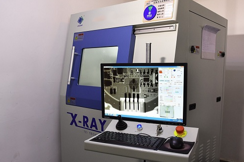
X-ray Inspection
6.3 Debugging
(1)Common failure modes:
- Power Issues:
Symptoms include: no power and voltage drops.
Check the outputs of regulators, diode orientations, and fuse continuity.
- Signal Integrity Issues:
Symptoms: Glitches, EMI.
Debugging: Add capacitors to decouple noise and reroute noisy lines.
- Firmware/Software Bugs:
Symptoms: MCU freezes, communication errors.
Debugging: Review code/logs and use JTAG debuggers.
(2)Step-by-Step Debugging Process:
- Identify the problem:
Divide the PCB into functional blocks (power analog, digital).
Identify the problem:
Divide the PCB into functional blocks (power analog, digital).
Test each block separately.
Test each block separately.
- Signal Tracing:
Follow the signals as they move from input to output using an oscilloscope.
- Component-Level Checks:
Replace suspected faulty parts (e.g. swapped ICs).
- Environmental Testing:
Test the product under extreme conditions, if applicable (temperature and vibration).
7.PCB Assembly FAQs
8.Summary
PCB assembly can be a complex and fascinating process. The PCB assembly transforms an electronic circuit into a working component. To create high-quality boards, each step in the PCB assembly is vital. The initial design check is followed by the assembly process, quality control, and verification. In today’s technologically-driven world, PCB assembly skills are essential for anyone working on a high-volume electronic prototype.
Latest Blog

Contact Info
Phone: +86-755-82882936
Email: [email protected]
WhatsApp: +86-13570802455
Wechat: +86-13570802455
Address: 2nd floor,D Bldg.,Electric Link Technology Bldg.,Gongming,Guangming New Dist.,518106 Shenzhen, China