Flexible PCB Board, Proto PCB Board, PCB Board Industry Development and Implementation
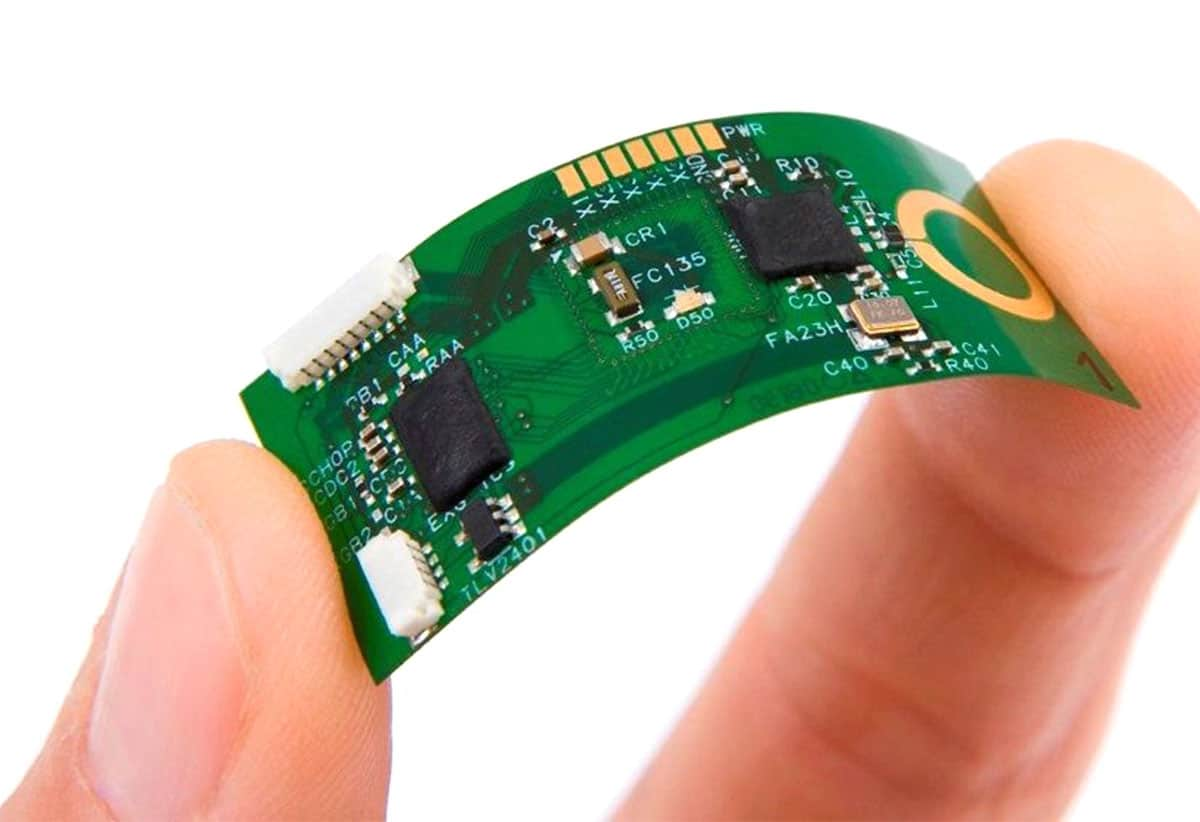
Table of Conent
Table of Conent
This article examines three key areas of PCB technology today: Proto PCBs and PCB boards fabrication. Their unique characteristics, their applications and the impact they have on businesses are explored.
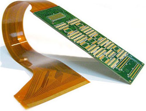
Flexible Circuit Boards: A new twist on Conventional Circuit Boards
Flexible printed circuit board, also called flexible PCBs (Flex PCBs), is the latest innovation in printed circuit board manufacturing. These are similar to rigid PCBS but made from flexible substrates such as polyester or polyimide films. They can also be bent, folded and conformed to various shapes.
Design and Construction
The core of a Flexible PCB consists of a thin transparent layer that is used to print or erase flowing errors. This substrate is usually made from materials like polyimide, which have excellent chemical and thermal resistance. Copper is the most common conductive copper. It can be used in various processes, such as electrode positioning or lamination.
There are several steps involved in the manufacturing of flex PCBs:
1. Design and System Architecture
2. Preparation and installation of the substrate
3. The Conductive Level Application
4. Light-resistance coatings and reflection
5. Engraving conductive patterns
6. How to apply a solder mask or coverlay
7. Final Inspection and Testing
Flexible PCBs: Advantages
1. Space Saving: Flexible PCBs are easily bent or folded into any compact shape, making it possible to create compact devices.
2. Weight reduction: Due to its low volume, they are used by portable electronics, computers, and the aerospace industry.
3. Dynamic flexibility: They are able to withstand repeated bending, or periods of bending. This makes them suitable for mechanical movement.
4. Reduced failure points: Less connections are needed, which reduces the number of potential failure points.
5. Enhanced Thermal Management: The Flex PCB’s thin profile allows for a better heat transfer.
6. 3D design capabilities: Flex PCBs allow for creative, three-dimensional circuit design that is not possible with rigid boards.
Flexible PCBs
Flex PCBs are becoming more popular in a variety of industries due to their flexibility.
1. Consumer electronics: Mobiles, tablets and other wearable devices use destructible storage systems.
2. All vehicles: Flex PCBs are used in the dashboard display, sensors and control systems.
3. Medical devices: Their ability to conform to various dimensions makes them ideal as implantable devices and diagnostic instruments.
4. Satellites and Flight Instruments: The flexibility and reliability of Flex PCBs is essential for satellite systems and flight instrumentation.
5. Industrial Equipment: Flexible PCBs are used in industrial equipment, such as robotics, control system, and sensors to monitor harsh environments.
Future Developments and Challenges
Flex PCBs are not immune to certain challenges, despite their many advantages. The cost of materials and manufacturing processes are higher for rigid PCBs. In order to make flex PCBs it is necessary to have a specialized understanding of the design process that takes into account stress points and functionality as the board bends or flexes.
Future flex PCBs will have improved durability, a greater number of layers which can be reliably manufactured, and newer materials that offer enhanced properties. Research is currently being conducted on stretchable PCBs that could also change the look of medical implants and wearable technologies.
Proto PCBs: Bridging The Gap Between Design and Production
Prototype PCBs are a major step towards the full-scale production of electronic devices. They bridge the gap between conception and full-scale manufacturing. Engineers and designers can use them to refine and test their designs before they are fully manufactured.
Prototyping is important in the PCB design process because of the following reasons:
1. Verfication of circuit design: Proto PCB allows designers to verify circuit design in physical form.
2. Detection of errors: It’s always better to detect errors at the beginning of the process. This will save you time, money and resources.
3. Optimizing: By using prototypes, the layout and the components as well as general performance can be “fine-tuned.”
4. Cost estimation: Prototyping is a great way to estimate the cost of the final production.
5. Investor presentations: These functional prototypes can be extremely useful when presenting your ideas to investors or other stakeholders.
Types and Applications of Proto PCBs
There are a number of ways to create a Proto PCB, each with its own advantages and use cases. This includes:
1. Breadboard prototyping: This involves using solderless boards for quick assembly and testing. This is not a PCB, but it’s often the first step of most prototyping projects.
2. Perfboard prototyping: This involves soldering the components on a board that has been predrilled with holes. This method is much more permanent than a breadboard. Changes are relatively easy to make.
3. Etched prototypes: These are created using chemical etching techniques, which you can perform at home or with a small professional service. These prototypes are more similar to final PCBs, but they’re usually limited to a dual or single layer structure.
4. CNC-milled prototyping: Computer Numerical Control (CNC) machines use eroding, which is a fast milling of copper away from a PCB board to generate prototypes for single-sided or double-sided boards.
5. 3D-printed Circuit Boards: This technology has not yet reached its full potential, particularly in the prototyping of PCBs with complex three-dimensional design.
6. Professional Prototyping servise: Prototyping services offered by PCB manufacturers include rapid prototyping, which is a service that allows for the production of small quantities of high-quality multi-layer PCBs in a near-final form.
Process of Prototyping
The prototyping process usually follows the following steps:
1. Schematic design: Using CAD software, a detailed circuit diagram can be obtained.
2. PCB Layout: The translation of the schematic to a physical board layout, taking into account parameters such as component placement and trace routing.
3. Design rule check: This is a way to ensure that the design meets the constraints of the manufacturing process as well as the electrical requirements.
4. Fabrication of prototypes: The actual fabrication of a physical PCB using any of the above methods.
5. Component assembly: The mounting of electronic components on the board.
6. Test and debug: Verifying that the prototype is actually working and fixing any issues.
7. Iteration: The process of improving a design on the basis of test results and repeating until it meets its purpose.
Proto PCBs: Advantages
1. Early identification and resolution of problems reduces the cost-cutting mistakes made in mass production.
2. Adding a step to prototyping saves you time by avoiding major redesigns later in the process.
3. Prototyping is cost-effective if the investment in prototyping can be offset by optimized designs and fewer production errors.
4. Iterative prototyping results in improved designs and a higher quality final product.
5. The prototyping process allows you to easily test out different components, layouts, and designs.
Challenges of Proto PCB Development
Proto PCBs have many advantages, but they also present challenges. These include:
1. Time factor: Rapid prototyping can sometimes be a bit hurried. It puts pressure on both the designer and manufacturer to deliver the product in a timely manner.
2. Cost: Although prototyping costs less in the grand scheme, it can be quite expensive when dealing with a design that has multiple layers in small amounts.
3. Functionality is Limited: The prototypes may not be able to represent the final product in terms of durability and performance.
4. Scaling Issues: What works on a prototype may not work flawlessly in a production environment.
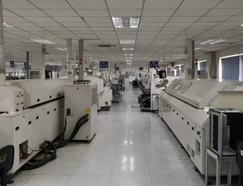
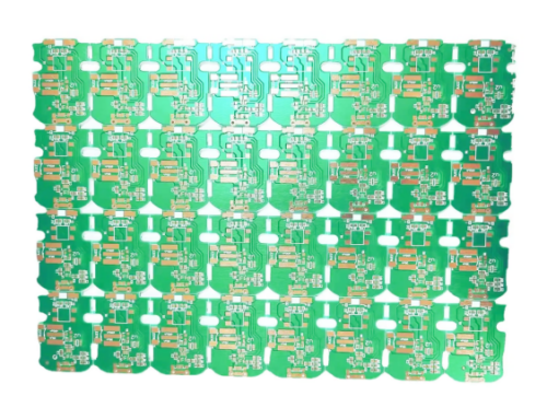
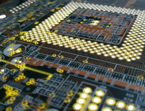
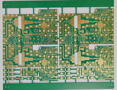
PCB Board Fabrication: The Art and Science of Bringing Designs to Life
PCB Board Making is the process of creating a printed circuit board from a designer’s idea. Such a complicated process involves many steps and demands manufacturing in an advanced, technology-intensive, precise, and detailed way to establish the required quality of PCBs.
PCB Fabrication Process
1. Design and File Preparation
These files are usually in Gerber format. These files contain the information needed for fabrication including:
• Dimensions and board outline
• Copper layer layouts
• Details on silkscreen and solder mask
• Drilling locations and sizes
• Information on stacking for multi-layer board
2. Material Selection
The performance of the PCB is dependent on the choice of base material. Materials that are commonly used include:
• FR-4: Common PCB with glass reinforced epoxy laminate.
• Polyimide: used for high-temperature applications, flex PCBs and other conductive materials.
• Ceramics: High frequency and high power ceramics.
• Teflon: Teflon can be used to make high-frequency microwaves.
3. Inner Layer Processing (for Multi-Layer PCBs).
• The copper-clad laminate has been cleaned and then covered with a resist.
• Photoresist is used to image the circuit pattern onto the photoresist.
• The circuit pattern is created by removing the uncovered areas.
• The copper that is exposed on the surface of the circuit board is removed by etching.
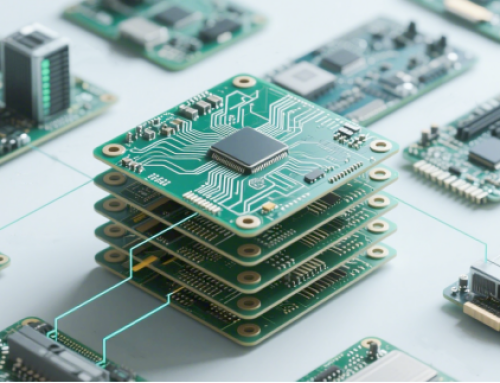
4. Layer Bonding
• Prepreg (or pre-impregnated material) is used to bond layers together in multilayer PCBs. This keeps the layers stacked one on top of another.
• The board is formed by pressing the stack under high temperature and pressure.
5. Drilling
• Holes for mounting, component leads and vias are drilled.
• Computer-controlled drilling machines allow for precise hole size and placement.
6. Copper Plating
• The entire board is coated with a thin copper layer, including the hole walls.
• This creates electrical connections in between the layers.
7. Outer Layer Imaging
The outer layers, similar to the inner layer, are imaged and then etched to produce the final circuit pattern.
8. Use Solder Mask Application
To cover copper traces on solder bridges, a layer of solder-mask, typically green but can be any color, is applied during assembly.
9. Surface Finish
Different finishes are available to protect exposed copper and enhance soldebility:
• HASL: Hot Air Solder Leveling
• ENIG: Electroless Nickel Injection Gold
• OSP: Organ Solderability Preservation
• Immersion Tin and Silver
10. Silkscreen Printing
The board can be marked with logos, component designations and other desired marks by applying white epoxy ink.
11. Electrical Testing
Checking continuity and isolation of the trace on the board.
12. Cutting and profiling
De-paneling: This is the process of separating individual PCBs and their panels, as well as cutting any slots or special features.
13. Final Packaging and Inspection
Before shipping, all final boards are visually and operationally checked.
Advanced Techniques for Fabrication
PCB fabrication techniques are evolving as the electronic world does:
1. HDI: HDI uses fine lines and microvias to increase circuit density.
2. Embedded components: Passive components, such as capacitors and resistors, can be fitted into the layers of a board to save space.
3. Rigid/Flex PCBs: By combining rigid and flexible sections on one board, it is possible to create more three-dimensional designs.
4. 3D Printed Electronics: This is a concept that has just begun. 3D printing is aimed at developing custom PCB solutions with very odd geometries.
PCB Fabrication Challenges
1. Miniaturization: PCBs must be able to accommodate smaller components and tighter tolerances as devices continue to shrink.
2. High-Speed Design: Take care when fabricating boards for high-frequency application, taking into consideration signal integrity and impedance.
3. Environmental Concerns: The PCB Industry is actively working to develop environmentally friendly manufacturing processes, materials and products.
4. Cost pressures: The eternal challenge–particularly in high-volume production–is maintaining the quality level at the best cost point.
5. Complex designs: Multilayer circuit boards that combine RF and digital technologies, for example, require highly sophisticated manufacturing processes.
Conclusion
PCB innovations are constantly changing, driven by the rapid rate of change in the hardware sector. Flexible PCBs expand the possibilities of device design, resulting in smaller and more flexible products for various businesses. Proto PCBs continue to be a crucial part of creating this plan, as it allows an originator to formulate out their thoughts and reduce risks before full-scale production. The PCB boards have been developed to accommodate the increasing demands of the miniaturized and more complex electronic devices.
It is important to introduce new innovations, like 3D printing or inserted components. These will change the look of a PCB and reveal previously unimagined possibilities of electronic design and functionality.
Engineers and architects who are able to understand adaptable PCBs, take advantage of prototyping and thus be updated on the latest manufacturing procedures will be able plan cutting-edge gadgets which extend the boundaries of what’s possible in the hardware world.
Latest Blog

Contact Info
Phone: +86-755-82882936
Email: [email protected]
WhatsApp: +86-13570802455
Wechat: +86-13570802455
Address: 2nd floor,D Bldg.,Electric Link Technology Bldg.,Gongming,Guangming New Dist.,518106 Shenzhen, China