Leading PCB Board Manufacturers, Top PCB Board Fabricators, and Innovative Circuit Board Design
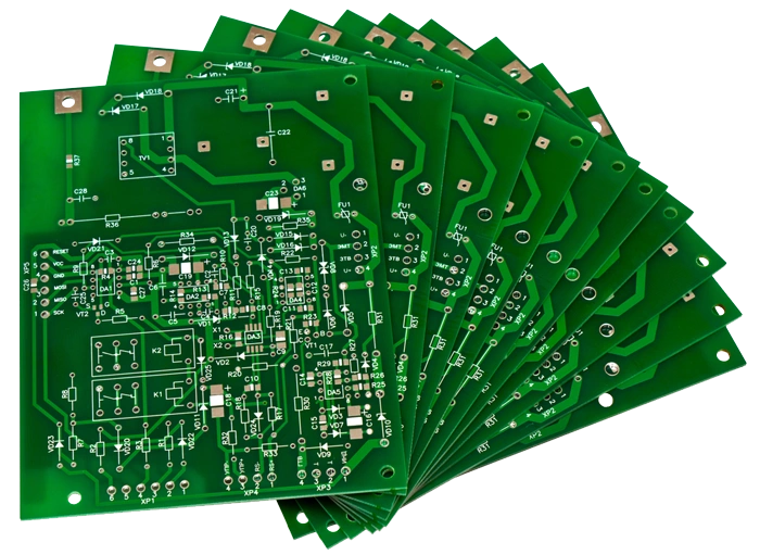
Table of Conent
Table of Conent
Printed Circuit Boards are the backbone of modern gadgets. They provide mechanical support and connect electronic components via conductive paths. PCB sheets are made with precision, advanced equipment, and specialized knowledge. This article will delve into the worlds of PCB manufacturing, plan forms and PCB makers.
Introduction of PCB Fabrication and Design
PCBs are used in virtually every electronic device, from simple contraptions to complicated aviation systems. The PCB is a flat board with copper tracks. It is used to mount components such as resistors and transistors.
Plan, creation and assembly are the steps in the journey of a PCB. PCB producers and designers must ensure that their products are not only useful, but also meet the highest industry standards for toughness and safety.
This guide covers all aspects of PCB preparation, from planning to making. It focuses on the best practices, the latest innovations and the major players in the PCB industry.
PCB Manufacturing: From Concept to Reality
1. Understanding PCB Fabrication
The PCB manufacturing process is used to create the physical circuit boards that are the platform for electronic components. The preparation of the creation includes key stages such as:
• Planning and Design Approval: A few weeks before the start of generation, the plan was carefully checked for irregularities or errors. The PCB will be produced according to the design details provided by the designer.
• Fabric Substrate Determination: The base fabric or substrate is normally made from fiberglass, reinforced epoxy tar or another protective fabric. The most common substrate is FR4, as it offers a good balance of electrical execution and durability.
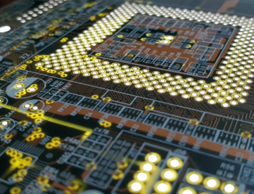
• Copper Cladding: Most PCBs have layers of copper on the surface. A copper layer is applied to the substrate and then a circuit design is transferred onto it using a photolithography handle.
• Etching: Unwanted copper is removed using a chemical preparation called carving. The circuits that are needed to form the electrical connections remain intact.
• Drilling: Gaps must be drilled to accommodate through-hole components (vias) or interlayer connections. Copper is plated over these gaps to create conductive connections.
• Application: A protective layer, known as a “patch cover”, is attached over the copper leads to leave the association points (cushion) exposed. The patch cover anticipates short circuits and provides a visual guide during component placement.
• Silkscreen printing: This layer has images and content that provide a way to distinguish between components, such as proof marks or portion numbers.
• Surface finishing: Different surfaces finishes such as HASL (Hot Air Solder Leveling), ENIG(Electroless Nitino Immersion Gold) or OSP (Organic Solderability Preservation) are applied to enhance solderability and protect exposed copper.
2. Testing and Quality Control in PCB Fabrication
After the manufacturing process is complete, the PCBs are thoroughly tested for quality and execution. Testing strategies include the following:
• Automated Optical Inspect: AOI frameworks inspect the surface of the board for any defects in the circuit design such as broken leads or misalignments.
• Electrical Test: The PCBs are tested electrically to ensure that they do not contain any open circuits or short circuits.
• X ray Inspection: High-end PCBs are inspected with X rays. This is especially true for those with multiple layers.
Circuit Board Plan: Where Innovating Begins
1. The Importance of PCB Design
The PCB plan is the first stage in the lifecycle a printed circuit. The quality, reliability, and usefulness of an electronic gadget are all dependent on the PCB plan. A poor plan can cause flag impedances or overheating of the device.
The designers use a specialized computer program for the layout of the circuit. They place all the basic components, and plan the copper leads that will connect them. This handle requires an in-depth understanding of both electrical behavior and the physical limitations of the device.
2. The Key Steps of PCB Design
a. Schematic Capture
A schematic is the first step of PCB design. It’s a diagram that shows electrical connections. The schematic is constructed using CAD instruments (Computer Aided Plan), which show how components such as capacitors, chips, and resistors are connected.
b. Component Placement
Components must be placed on the board once the schematic is complete. It is important that the creators adjust electrical performance to physical limitations. Consider components like flag sharpness, warm administration and mechanical stretch.
• Signal Acuity: High speed circuits such as those used in broadcast communications require unusual considerations to be made to the lengths and positions to anticipate impedances.
• Thermal Administration: Proper component arrangement will help to keep components warm and prevent them from overheating.
• Mechanical Push: Components should be set up to minimize mechanical pushing during operation. This could lead to wear and failure.
c. Routing
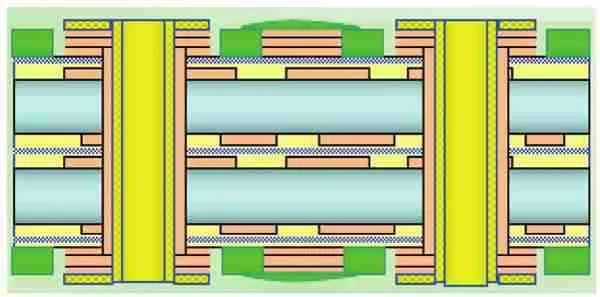
Routing is the process of drawing the copper lines that will connect the components. The architects must arrange these copper follows in a way that they do not cross over. The multi-layer PCBs that contain multiple stacked copper layers allow for more complex routing.
d. Design Rules Check (DRC)
The plan is then subjected to a Design Rule Check, or DRC. This ensures that the plan meets industry benchmarks as well as producer limitations. These rules include viewpoints such as the minimum follow width, dividing follows and the estimation of penetrated gap.
e. Analysis and Reenactment of Flags
The signal simulation devices help creators to predict how a circuit will work in real life. These devices can simulate variables such as flag reflection, control transmission, and crosstalk. This allows creators to make changes in the circuit.
3. PCB Plan Computer Program Tools
The design of a PCB is a complex process that requires a number of natural and effective program tools. Some of the most popular PCB design program bundles are:
Altium Architect is a highly advanced tool that combines PCB layout, schematic capture and simulation in one package. Due to its powerful features, it is widely used in professional situations.
• Hawk: Hawk is popular amongst both experts and specialists. It has a large library of components, and it is highly customizable.
• KICAD: A free open-source alternative that is comparable to Altium or Hawk, but offers similar functionality. It is a popular choice for small businesses and new companies.
• OrCAD: OrCAD is a professional-grade tool that offers a wide range of features and reenactment abilities.
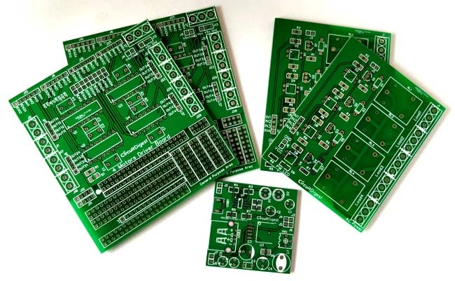
PCB Board Makers: Turning Designs Into Reality
1. PCB Makers: Their Role
PCB producers are responsible for transforming a plan or design into a tangible item. The PCB producer uses the PCB architect’s plan, plans the materials and uses advanced fabricating hardware.
The manufacturers offer a wide range of services, from design generation to large-scale manufacturing. Many producers also offer assembly services, where they place and patch components on the PCB to make a complete electronic device.
2. Considerations to Make When Choosing a PCB Manufacturer
The success of any hardware project depends on selecting the right PCB manufacturer. Here are some key factors to consider:
• Capabilities: Different producers specialize in different types of PCBs such as multi-layers, single-layers or adaptable sheets. You must choose a manufacturer that can meet the specific needs of your design.
• Turnaround time: This is essential for projects that are time-sensitive. Some producers provide assisted administrations at an additional fee.
• Quality Assurance: Ensure that the producer is putting in place a solid quality assurance plan, including review and testing for each stage of production.
• Cost: While cost is always a consideration, the cheapest option is not always the best. While high-quality PCBs are more expensive upfront, they can save you money in the long term by reducing the chances of failures and absconds.
• Certifications: Look for manufacturers with ISO 9001 or IPC benchmarks (Organization for Printed Circuits), which demonstrate their commitment to quality.
3. PCBs for Prototypes Versus Production PCBs
Most PCB manufacturers offer two main administrations: prototype and generation PCBs. The prototype is the preparation of making a small clump PCBs to test and approve. Generating, on the contrary, is the process of fabricating larger quantities for commercial use.
a. PCB Prototype
The prototype PCB is essential for verifying the plan and ensuring it will work as expected. These PCBs can be made in small quantities, allowing the originator to identify and correct any problems before moving on to full-scale production.
The turnaround time for prototype administrations is usually faster and they are more flexible in terms of changes to plans.
b. Production of PCBs
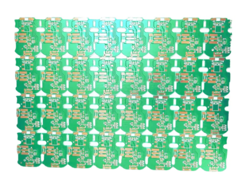
After the model is approved, generation follows. It involves fabricating PCBs at large quantities, usually thousands or millions depending on the application. To ensure consistent execution, PCBs produced in the future must adhere to strict quality standards.
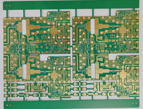
What Exactly Is a Printed Circuit Board?
A Printed Circuit Board is a board which mechanically supports electronic components and interconnects them electrically. It uses conductive tracks or hail takes after carved out of copper sheets, secured to a nonconductive substrate. PCBs play a crucial role in the operation of electronic devices, as they provide the means for components to communicate and signals to flow.
PCB Types
PCB manufacturers deliver different types of sheets depending on what gadgets they are going to be used in. Here are some common types:
1. Single-Layer PCBs: These are suitable for simple devices, as they contain only one layer of fabric.

2. Double-Layer PCBs: These boards feature two layers of conductive fabrics, allowing for more complex designs.
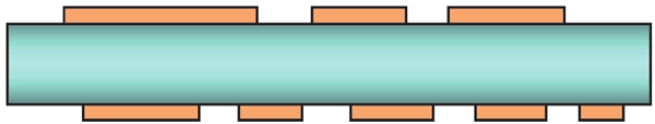
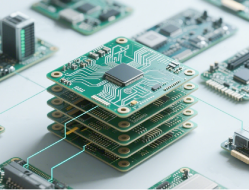
3. Multi-Layer PCBs: These boards have three or more layers of conductive material and are used in advanced gadgets which require high performance in small spaces.
4. Rigid PCBs: These are made from a strong substrate fabric that is outlined in a rigid manner.
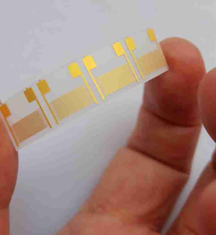
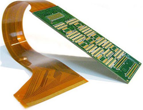
5. Flexible PCBs: These are made from materials that can be twisted without breaking.
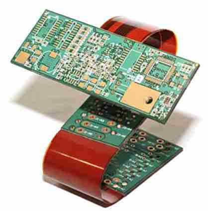
6. Rigid-Flex Circuit Boards: Combination of rigid and flexible circuits that allows for dynamic bowing and adaptation within the design.
The PCB Fabrication Process
PCB fabrication is a process that involves several stages from planning to testing. The following is a simplified version of the usual steps that a PCB manufacturer follows:
1. Design: A PCB plan is created using a specialized program such as Altium or Hawk. This plan includes the location of the conductive traces and the path of the components.
2. Printing Design: Once the design is complete, it is printed on the copper layer. This can involve printing different layers in alignment, depending on how complex the design is.
3. Etching: Unwanted copper is removed from the board. The copper that forms the electrical connections follows.
4. Drilling: Gaps, such as those for resistors or capacitors, are bored in the PCB. This step is crucial for multilayer PCBs to ensure a network between the layers.
5. Application of Plating and Solder Mask: The gaps are plated and a patch is attached to the copper leads in order to prevent short circuits during soldering.
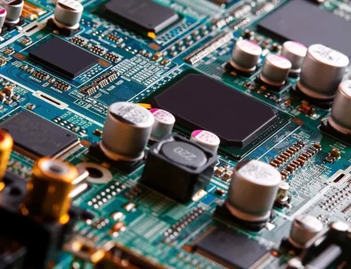
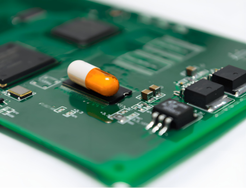
6. Component arrangement and patching: The electronic components are placed on the board and then fastened to the copper traces.
7. Quality Control: The PCB is tested thoroughly to ensure its capacity as planned. It may include visual checks, electrical tests and useful tests.
Why It Is Important to Choose the Right PCB Manufacturer
The choice of the PCB manufacturer is crucial and can affect the success of an item. Consider these factors when selecting a Printed Circuit manufacturer:
1. Quality control: It is important to ensure that the producer follows strict quality control procedures. Look for ISO-certified producers who have a proven track record in delivering high-quality goods.
2. Capabilities: Different producers specialize in different kinds of PCBs. Choose a manufacturer who has experience in the type of board that you need, whether it is a simple single-layer PCB or a multilayer or flexible PCB.
3. Lead time: Time-to-market is a fundamental in many businesses. Choose a manufacturer that can meet the timelines you need, whether it’s for quick-turn models or mass production.
4. Cost: While fetched should not be as thought, it is important to find a manufacturer that offers competitive pricing without compromising quality.
5. Customer Bolster: A good PCB manufacturer should provide amazing customer bolster. This includes specialized assistance during the planning stage, clear communication throughout the manufacturing process, and after sales service.
Conclusion
There are many companies that offer a variety of services to suit the requirements of different businesses. If you are creating an electronic gadget for a customer or a modern aviation system, selecting the right PCB manufacturer can make a huge difference in terms of quality and execution.
To remain competitive, the top manufacturers of the industry adopt new technologies and improve their processes. The demand for reliable, high-quality PCBs is increasing as the market for advanced electronics continues to grow. Partnering with the right manufacturer will help you ensure that your products are up to date and meet today’s high standards.
Latest Blog

Contact Info
Phone: +86-755-82882936
Email: [email protected]
WhatsApp: +86-13570802455
Wechat: +86-13570802455
Address: 2nd floor,D Bldg.,Electric Link Technology Bldg.,Gongming,Guangming New Dist.,518106 Shenzhen, China