Manufacturing test challenges for complex Printed Circuit Board Assemblys (PCBAs)
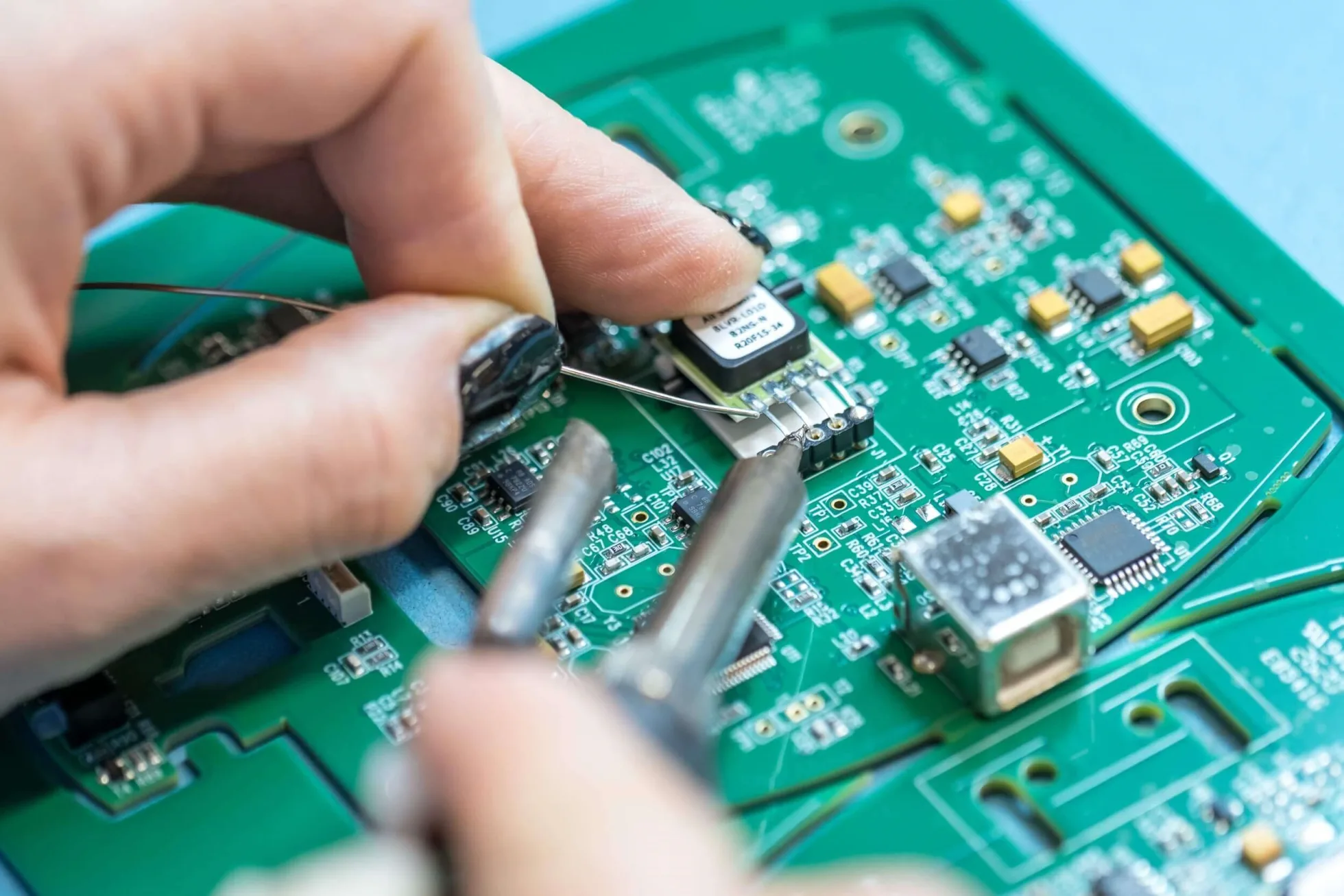
Table of Conent
Table of Conent
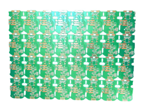
Printed Circuit Board Assembly is a fundamental viewpoint in advanced gadgets production, where components can be assembled onto a PCB for the purpose of making useful electronic gadgets.In the last few decades, PCB complexity has increased dramatically, posing new challenges to the manufacturing process.Modern electronic gadgets require less complex, but more useful, plans and a more predominant execution. This requires more modern PCBA testing methods.
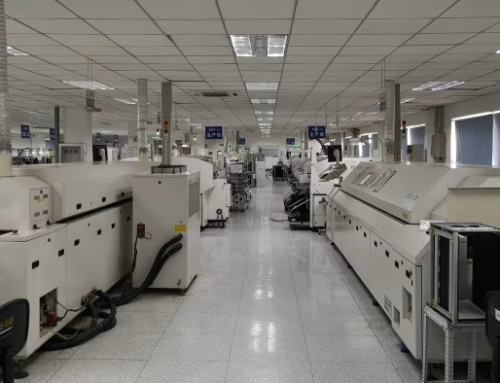
PCBAs are composed of many stages including planning, component selection, placement, patching and testing.Testing is important as it helps to identify any mistakes that might have occurred during manufacturing.The testing process for complex PCBAs must take into account complex designs, high component thicknesses, multi-layered sheets and the need for rapid prototyping.This article discusses the challenges associated with testing complex PCBAs as well as possible solutions to these challenges.
The Increasing Complexity Of PCBs
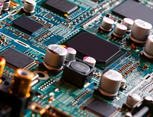
Miniaturization of Tall Component Density
Miniaturization is one of the most notable trends in modern hardware.Customers and businesses expect greater utility from gadgets as they get smaller.PCBs have thicker components, so more components can be crammed onto one board.As components become smaller and more closely separated, manufacturing abandons are likely to increase.
The conventional methods of testing such as visual review and manual testing have not been successful.It is difficult to reach individual parts of the board due to their size and proximity.It is necessary to use advanced testing methods such as Automated Optical Inspections (AOI) and X-ray assessments in order to identify issues without coordinating physical contact.
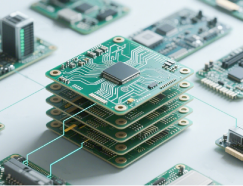
Multilayer PCBs
Many advanced PCBs have multiple layers in addition to their miniaturization.Multi-layered PCBs allow for a more complex circuitry, and enable higher utility in a smaller impression.The added complexity can be a challenge during the testing phase.Multi-layered sheets make it more difficult to reach and test the inner layers. This requires advanced, non-invasive testing techniques.
Complex Network Functionality
The number of components and interconnections increases exponentially in complex PCB assemblies.Communication is required between components such as memory chips, controllers, chip, and sensors.In the PCBA’s utilitarian test, it is important to confirm that the components are working together in harmony.It is important to ensure that the signals are transmitted accurately over the board and to address any issues related flag acuity, electromagnetic interference (EMI), or warmth administration during testing.
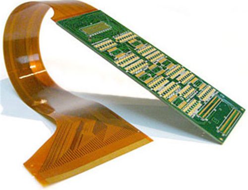
Flex-Flex PCBs
In some applications, like smart phones, medical devices, or aviation parts, flexible PCBs or rigid-flex designs are used to satisfy the need for lightweight, bendable and extremely tough circuit sheets.Due to their physical properties, these plans pose special testing challenges.Flexible circuits are difficult to test because they can turn and twist.
PCBA Testing Types
In order to meet the challenges associated with complex PCBs the producers use a combination testing strategies in order to ensure the final item meets the quality and unwavering measures.These include:
1.In-Circuit Testing (ICT)
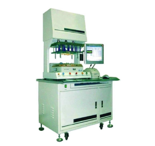
ICT is one of PCBA manufacturing’s most common testing methods.The board is tested for electrical parameters such as coherence, capacitance and resistance.ICT is a powerful tool for detecting component-level errors, such as short circuits, open circuits and incorrect component placement.
ICT becomes difficult for PCBs that are complex due to the lack of test targets.The number of test points decreases as sheets become thicker and more multi-layered. This reduces the effectiveness of ICT systems.
2.Automated Optical Inspection (AOI)
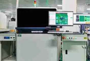
AOI uses cameras to take high-resolution images of the PCB. It can then be used to identify any omissions, such as missing components, patches, or parts.AOI, a non-contact test strategy, is ideal for PCBAs with high density and complexity. It doesn’t need physical access to the board.
AOI can be a powerful tool for detecting surface-level defects, but it struggles to detect issues in the inner layers, or patches joints that are hidden under components such as Ball Grid Arrays (BGAs).AOI may not be able to detect all defects on PCBs due to their complexity.
3.X-Ray Inspection
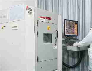
The X-ray test is a nondestructive strategy for producers to examine the inside of PCBs and components.This is particularly useful for identifying patch joint surrenders that are covered, like those found on BGAs and other surface-mount devices.The X-ray can also reveal issues such as voids, misaligned parts, and inadequate patch coverage.
The difficulty with X ray evaluation is the distance and the skill required to interpret the results.While X-ray assessment can provide valuable insight into difficult-to-detect snares, it may not be feasible for all manufacturers to include a scheduled step in their manufacturing plan due to the high upfront costs of the equipment.
4.Functional Testing
Functional testing involves running the assembled PCB under a simulated working environment in order to verify that it functions accurately.This test is used to check if the different components of the board work as expected under real-world conditions.This is particularly important for PCBAs that have advanced chip, sensor, and communication interfaces.
It is the setup that poses the biggest challenge to useful testing.It can be expensive and time-consuming to create a test environment that is suitable for complex gadgets.Investigating utilitarian problems can also be difficult, since the cause of the problem may not always be obvious, and require extensive troubleshooting.
5.Boundary Filter Test
Based on the IEEE 1149.1 standards, boundary filter testing allows for the testing of individual components and their interconnections without the need for physical testing focuses.This is particularly useful for testing highly complex sheets, where physical access is limited.
The boundary filter test can identify many types of abandons. However, it is limited to components that support the boundary filter standard.Coordination boundary test into the planning stage can require additional resources and planning.
Common Manufacturing Defects in Complex PCBAs
1.Open Circuits
When there is a break along the electrical path, it can cause an open circuit. This happens when current starts to flow.It can be caused by a lack of patching, a broken follow, or faulty component alignment.Open circuits are more difficult to identify in multi-layered sheets, where the defect may occur in an inner layer. Visual assessment is therefore ineffective.
2.Brief Circuits
A short circuit occurs when two electrical paths that are not intended to be in contact come into contact. This causes an excessive amount of current to flow through the circuit.Overheating can occur, causing component failure or even damage to the entire board.The high component thickness increases the likelihood of short circuits in complex PCBs. This is because small patching mistakes or plan imperfections may cause unintended connections.
3.Cold Patch Joints
Cold patch joints are caused when the patch is not fully dissolved in the patching handle. This results in a weak association.Visually, these abandons can be difficult to detect as they might appear intaglio yet fall flat under operational stretch.Cold patch joints tend to occur in PCBs that have fine-pitch components, or BGAs. This is because it’s difficult to achieve the right scope of patching.
4.Component Misplacement
The chance of placing components off base area increases in extremely complex assemblies, especially when working with small, similar-looking pieces.Components can be lost in computerized situation machines due to programming errors or mechanical flaws.Loss of components can be a source of frustration and disappointment. They are difficult to detect without advanced assessment methods such as AOI.
5.Solder Bridges
When abundance patch is unintentionally associated with two adjacent components or cushions, a patch bridge occurs.This is common in PCBs with high densities, where dispersion between components is minimal.Patch bridges are prone to short circuits, and can be difficult to detect in densely populated areas of the board.
Test Challenges for PCBA Technologies
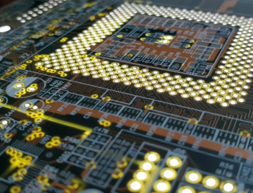
1.Ball Grid Arrays
BGAs have been widely used in advanced gadgets because of their ability to provide a large number of I/O connections in a small area.BGAs present a significant challenge during testing, as their patch joints are located underneath the component. This makes them inaccessible for conventional or visual testing methods.
The most effective way to detect surrenders is through X-ray analysis, but this is expensive and requires special equipment.Due to the compactness of BGAs, it is difficult to revamp a BGA that has been deemed inadequate. It is therefore important to identify any surrenders as early as possible in the manufacturing process.
2.Surface Mount Devices
Surface mounting technology (SMT), allows components to be placed directly on the PCB surface without the need for through-hole lead.SMT is a great way to create compact, effective plans. However, it can be challenging when it comes to patching and testing.
SMDs often have fine-pitch lead wires that need to be fastened precisely in order to avoid surrenders like patch bridges and inadequately patched scope.ICT testing may not be suitable for fine-pitch components. Instead, they should use AOI, an X-ray or another non-contact method.
3.High-Frequency High-Speed Circuits
In more advanced applications such as broadcast communication, aviation and automobile frameworks, PCBs must support high-frequency, high-speed signals.In these applications, ensuring flag acuity is a challenge. Indeed, even small abandonments or format problems can cause flag interference or degradation.
Tests of high-frequency circuits require specialized hardware, as well as a thorough understanding of parameters like impedance and flag reflection.The complexity of high-speed systems makes it more difficult to test them, since they can be more complicated.
4.Thermal Management
Thermal management is a fundamental aspect of PCBA testing, especially in applications that use high-temperature control.Thermal management is another important aspect of testing complex PCBAs, particularly in applications where tall control utilization produces critical heat.
In order to test for warmth, it is necessary to ensure that heat is properly managed through the use of heatsinks and warm vias.Infrared and warm imaging cameras are often used to identify hotspots during testing.
Solutions for Manufacturing Test Challenges
1.Design for Testability
The best way to overcome testing challenges with complex PCBAs, is to integrate Design for Testability standards (DFT) into the PCB planning stage.DFT involves planning the board for testing, ensuring that it has open components and a legitimate format for robotic inspection.
DFT can include including test cushions, ensuring that basic signals are present for boundary check tests, and optimizing format to minimize impedances.Producers can reduce the likelihood of failures by planning the board from the beginning with testing in mind.
2.Automated Test Equipment (ATE)
Automated test equipment (ATE) is increasingly used to test complex PCBAs. This is especially true in high-volume production.ATE systems are capable of performing multiple tests simultaneously, providing a comprehensive range for electrical and useful parameter.ATE is also capable of performing stretch tests, ensuring that the board can function reliably under different natural conditions.
While ATE frameworks can be expensive, they can reduce testing time and increase throughput. This makes them an attractive alternative for PCBA producers who produce complex PCBAs.
3.Advanced Imaging Techniques
Producers can use advanced imaging strategies like 3D AOI and 3D X ray review to overcome the limitations of conventional review strategies.These strategies allow for a closer look at the board and can reveal hidden absconds which may not be obvious in 2D images.
3D X ray analysis can reveal defects in the inner layers or parts hidden under other components.These strategies are expensive and require special equipment, but they can be a great way to find flaws in complex PCBAs.
4.Continuous Monitoring and Real-Time Feedback
In PCB production, real-time input and non-stop checks can help identify absconds before they occur, which reduces the time spent on redesign and manufacturing.Sensors and data collection systems can be integrated into the production line to track parameters like temperature, fixing conditions and exactness of situation.
The real-time data can be used to change the manufacturing process on the fly. This will allow the sheets to pass through the testing phase with fewer defects.
Conclusion
Testing complex PCBs is a challenging process, particularly in the manufacturing stage.Conventional testing strategies became less effective as sheets became more complex, with increased component thickness, multiple layers, and advanced functionalities.For high-quality production, manufacturers must adopt advanced testing strategies, such as AOI (Aperture On Image), X-ray review and boundary check testing.
Design for Testability standards (DFT) can be incorporated into the planning stage to reduce the testing challenges associated with complex PCBAs.Automated Test Equipment, advanced imaging strategies and real-time input systems can improve the testing plan, ensuring that errors are detected early and efficiently.These challenges can be addressed by producers to improve the quality and execution of products while reducing costs associated with redesign and field failures.
Latest Blog

Contact Info
Phone: +86-755-82882936
Email: [email protected]
WhatsApp: +86-13570802455
Wechat: +86-13570802455
Address: 2nd floor,D Bldg.,Electric Link Technology Bldg.,Gongming,Guangming New Dist.,518106 Shenzhen, China