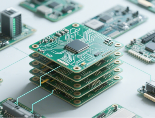
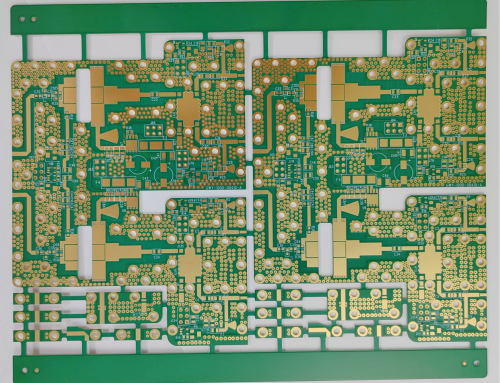
PCB Multilayer: PCB Panel V-Cut vs Stamp Hole
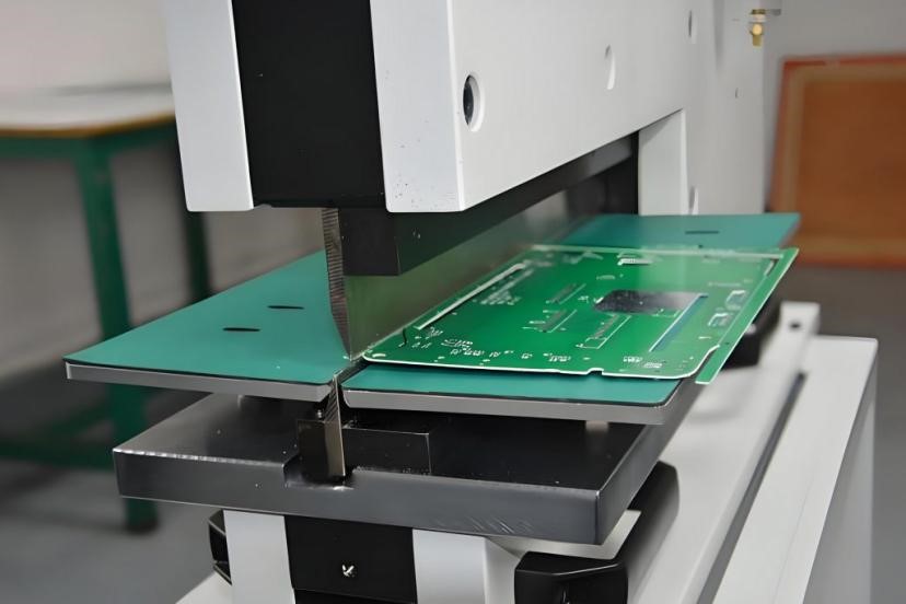
Table of Conent
Table of Conent
Circuit card panels are cut with V-shaped grooves by PCB Panel V-cut vs. Stamp Hole V-CUT, which makes it easier to remove the panels for further processing. In the meantime, stamp holes create a tiny hole at the panel’s edge to help the panels separate more neatly and steadily, which can improve signal transmission performance and use more space. Combining these two technologies guarantees product quality and dependability in addition to increasing production efficiency.
What is PCB V-CUT?
V-shaped grooves are cut out of printed circuit boards using the PCB V-CUT process, which is primarily used to make subsequent board separation operations easier. V-CUT involves cutting out a series of V-shaped notches in the printed board, and then breaking the board after applying the appropriate force, thus dividing the multilayer printed board into individual panels.
V-CUT’s Function and Significance
1. Boost Production Efficiency: When produced in large quantities, V-CUT can rapidly.
2. Reduce Material Waste: With V-CUT cutting, you can maximize the use of raw materials, reduce waste generation, and lower production costs.
3. Easy assembly: V-CUT makes separated small panels easy to assemble and solder, thus increasing production efficiency.
4. V-Cut is frequently used in multi-layer printed board volume manufacturing, particularly when a large board needs to be sliced into several smaller panels.
What Benefits and Drawbacks Does V-Cut Offer?
1. Benefits of V-Cut:
• Ease of Handling: After assembly, the V-Cut design makes it easier to separate SMT boards, preventing manual separation that could bend circuit cards and harm electronic components.
• Increased Productivity: When assembling two board edges, the efficiency of SMT placement lines and wave soldering can be significantly increased.
• Vast range of applications: V-Cut works well with standard circuit boards and can greatly increase productivity, particularly in mass production.
2. Drawbacks of the V-Cut:
• The inability to modify in the middle and the ability to only cut straight lines. It can only cut straight lines from one end to the other. It is not permitted to bend in the middle at a 90-degree angle or any other angle.
• High demands on the tools: The V-Cut tools’ material and manufacturing technique greatly affect the cutting outcomes. For instance, alloy inlaid V-Cut cutters increase the brittleness of the blade due to soldering, making it difficult to ensure the quality of the cutter and having a high breakage rate; high-speed tool steel V-Cut cutters, on the other hand, are not wear-resistant and require frequent replacement and sharpening of the tip, which affects productivity.
• PCB Thickness Limitations: V-Cut cannot be used with printed boards that are too thick or thin since the former are difficult to cut and the latter are brittle.
What is a Stamp Hole?
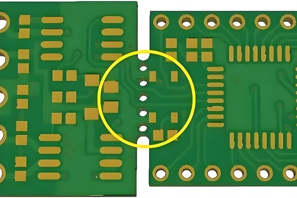
The little circuit cards that make up the array are connected together by a stamp hole in the motherboard panel, which also makes it simple to remove components from the PCB. Components can be removed without causing damage to the board since the perforated stamp hole splits when pressed down.
1. The Stamp Holes Serve the Following Specific Purposes:
• Attaching tiny PCB boards: Connections can be made through the stamp holes when several small circuit cards need to be connected and connectors are not available. Current can pass through the PCB and link to nearby boards thanks to the perforations.
• Power and Data Transmission: To facilitate communication between devices, stamped holes can transfer power and data between two distinct printed boards or devices.
2. The Following are Design Specifications for Stamp Holes:
• Number of Holes: Depending on the PCB design, the precise number of stamp holes required to join components may vary, however they are often utilized in groups of five.
• PCB Multilayer: V-cut vs. stamp hole PCB Panel Dimensions: Stamp holes typically have a diameter of 0.020 inches or 0.5 mm, depending on the PCB design.
• Hole Spacing: To avoid components being too near to one another and creating short circuits, stamp holes are normally placed 0.030 inches or 0.76 mm apart.
3. Here are Some Design Pointers for Stamp Holes:
• Sufficient Tie Tabs: The tie tabs must be robust enough to sustain the weight of the aforementioned components in order to preserve the integrity of the PCB.
• Avoid sensitive components: To prevent electrical shorts brought on by damaged tabs, stamp holes should be avoided near sensitive components.
• Spacing: To make it easier to install the components, there should be a 60–90 mm gap between two stamp holes.
What Benefits and Drawbacks Come with Stamp Holes?
1. Stamp Holes Have the following Benefits:
• Increased productivity: Stamp holes allow multiple small printed board to be connected together for production processing, thereby streamlining the production process and reducing costs.
• Ease of assembly and disassembly: Where a removable connection is required, such as in modular designs, stamped hole connections allow for easy assembly and disassembly for product maintenance and upgrades.
• Reduced Space Footprint: The stamp hole design significantly reduces the amount of space required, making it ideal for compact designs.
• Enhanced Signal Transmission Performance: Stamped holes make sophisticated multilayer board designs possible by shortening the signal path and lowering cross-talk and delays.
2. Stamp Holes Have the Following Drawbacks:
• Possible Cost Increase: The design of a stamp hole adds a certain amount of cost because of the need to reserve holes on the circuit card, and the size of these holes is included in the overall size of the circuit card.
• Breakout surfaces are difficult to manage: Breakout surfaces are difficult to precisely regulate, which can result in circuit damage or even junk. Stamp holes are separated by breakouts.
What Distinguishes a Stamp Hole from a V-Cut?
The main difference between a V-Cut and a stamp hole is their definition, use and application.
1. V-Cut: V-Cut is a pre-cut V-shaped demarcation line at a specific location on the circuit board, usually used to facilitate the de-paneling of assembled SMT boards. the demarcation line of a V-Cut is usually a straight line without complex curves or arcs, and it is suitable for the panel connection of a regular electronic board.
2. Stamp Holes: To join the process edges to the circuit board, a series of circular holes in the shape of stamps are punched into the board. It is mainly applied to boards that have asymmetrical shapes, like circles. Since V-Cut cannot realize this connection, stamp holes are mostly used in shaped boards.
How Can I Pick the Best PCB Depaneling Technique?
A lot of aspects need to be taken into account while selecting the best PCB depaneling technique, such as the PCB’s shape, manufacturing scale, budget, and product quality requirements.
1. V-CUT:
• Advantages: low cost, easy to operate, fast speed, suitable for regular shape PCB in a straight line.
• Disadvantages: only straight line off the board, not applicable to complex or irregularly shaped printed boards.
• Applicable scenarios: electronic cards have a fairly uniform shape and are appropriate for small and medium-sized mass production.
2. Stamp Hole:
• Benefit: It can offer greater space utilization and is appropriate for irregularly shaped electronic cards, like round or curved boards.
• Shortcoming: The cost is a little greater than with V-CUT, and some burrs might be produced during the separation process.
• Relevant Situation: Fits well with production that needs a lot of area and electrical boards with intricate or asymmetrical geometries.
3. Board Separation by Milling Cutter Type:
• Benefits: Suitable for PCBs of different shapes, smooth cutting edge, minimal stress, and ability to be separated into boards of any shape.
• Disadvantages: High initial cost, relatively complex equipment and operation.
• Applicable scenarios: suitable for cutting complex shapes of electronic card with high precision requirements.
4. Laser Board Separation:
• Advantage: high precision, suitable for electronic card with complex shapes and high precision requirements.
• Disadvantages: high cost, slow speed.
• Applicable scenario: suitable for small batch production with high precision requirements.
When selecting the board separation method, the specific needs of the product, production costs, production efficiency, product quality requirements and other factors should be considered to ensure that the most appropriate board separation method is selected. To satisfy the needs of various clients, ASSYPCB can flexibly apply a range of depaneling processes, including V-CUT and stamp holes, thanks to its experience and state-of-the-art equipment. Please get in touch with us for the best solution, regardless of how simple or complicated your PCB design is.
Latest Blog

Contact Info
Phone: +86-755-82882936
Email: [email protected]
WhatsApp: +86-13570802455
Wechat: +86-13570802455
Address: 2nd floor,D Bldg.,Electric Link Technology Bldg.,Gongming,Guangming New Dist.,518106 Shenzhen, China