Printed Circuit Board Assembly (PCBA): A Comprehensive Guide to PCB Board Assembly and PCBA Circuit Board
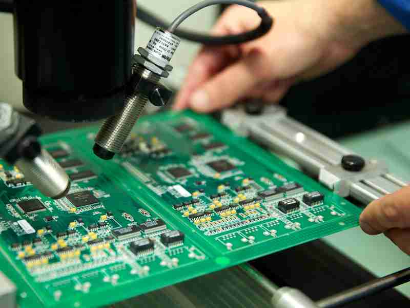
Table of Conent
Table of Conent
In today’s digitally driven world, electronic devices play an integral role in our daily lives. Whether it’s the Smartphone in your hand, the computer on your desk, or the car you drive, most of these present day gadgets owe their usefulness to one significant component: Printed Circuit Board Assembly (PCBA). From buyer gadgets to mechanical apparatus, PCBA is the heart of all electronic frameworks. In this comprehensive guide, we will delve into the world of PCBA, PCB board assembly, and PCBA circuit boards, explaining everything from the basics to more advanced aspects.
What Is a Printed Circuit Board (PCB)?
Before we get down to business and see how to assemble one, let’s know what basically a Printed Circuit Board, popularly called a PCB is. A PCB is a level board made from non-conductive fabric (such as fiberglass, composite epoxy, or other cover materials) that bolsters and electrically interfaces electronic components. It serves as the establishment upon which electronic components like resistors, capacitors, transistors, and coordinates circuits are mounted.
The PCB’s essential part is to course electrical signals between these components, guaranteeing they work accurately inside the bigger framework. Copper follows on the PCB act as wires, permitting the stream of power between different components without the required for physical wires.
The Advancement of PCBs
PCBs have advanced drastically over the past century. At first, electronic gadgets utilized point-to-point wiring, where components were straightforwardly associated by wires. This strategy was wasteful, time-consuming, and inclined to mistakes. The innovation of PCBs in the 1930s by Austrian design Paul Eisler revolutionized electronic plan by advertising a standardized and dependable way to mount and interface components.
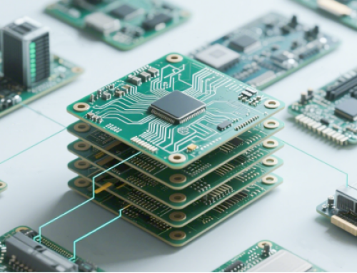
As innovation advanced, PCBs got to be more progressed. Nowadays, multilayer PCBs–where numerous layers of conductive fabric are sandwiched between protection layers–are standard in numerous applications, permitting for more compact plans and complex functionality.
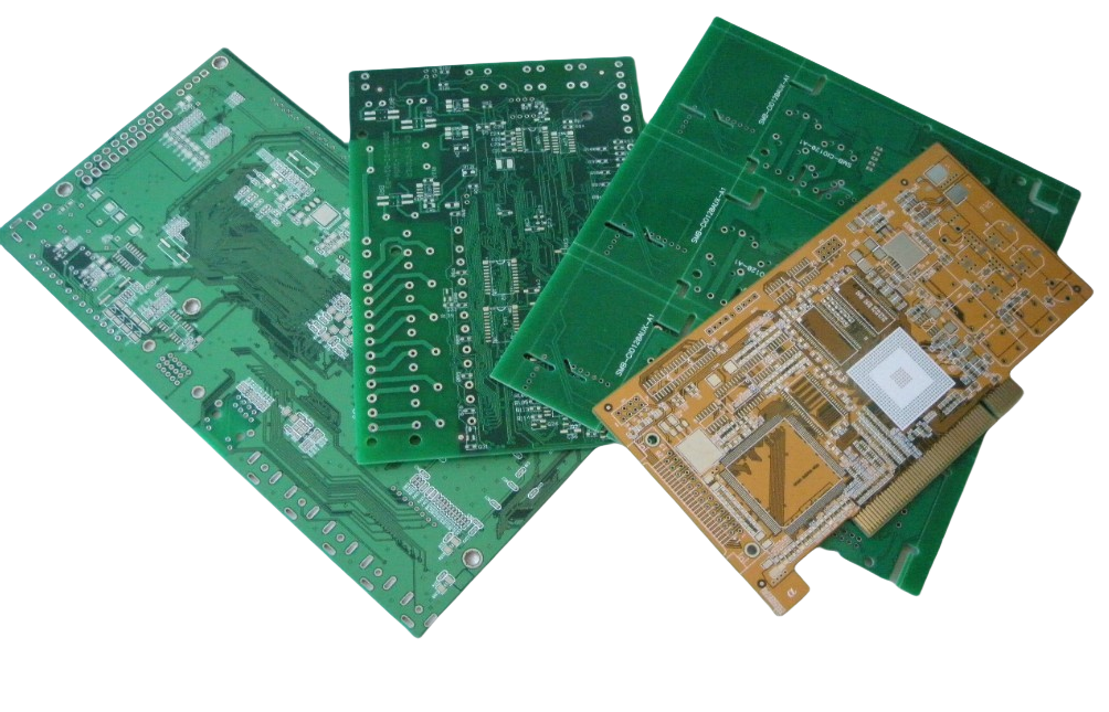
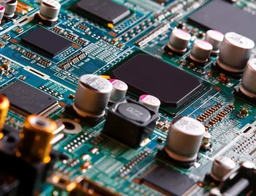
PCB Board Assembly (PCBA): What Does It Mean?
PCB Board Assembly (PCBA) refers to the process of soldering or assembling electronic components onto a printed circuit board to create a functional electronic circuit. While a bare PCB provides the foundation, the PCB Assembly (PCBA) process turns it into a working electronic device by adding the necessary components.
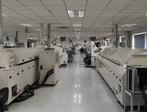
This prepare can include both Surface Mount Technology (SMT) and Through-Hole Technology (THT), depending on the complexity and prerequisites of the plan. PCBA is basic in businesses such as car, broadcast communications, aviation, and therapeutic gadgets, where accuracy and unwavering quality are paramount.
Steps Included in PCB Board Assembly
The prepare of PCB board assembly includes a few steps that must be carried out with awesome accuracy. Underneath is a breakdown of the key stages included in PCBA:
1. Plan and Preparation
The to begin with step in PCB assembly starts indeed some time recently the board is manufactured. The plan of the PCB, counting the arrangement of components, flag steering, and control conveyance, is significant to the execution of the last item. Engineers utilize specialized PCB plan program like Altium, Hawk, or KiCad to make the PCB layout.
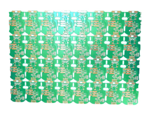
Once the plan is total, the Gerber records (which contain all the vital data for PCB fabricating) are created. These records are sent to the PCB producer, who produces the uncovered sheets. At the same time, a Charge of Materials (BOM) is arranged, posting all the components required for assembly.
2. Solder Paste Application
Once the uncovered PCB is prepared, the assembly handle starts with the application of patch glue. Patch glue is a blend of little metal balls (as a rule made of tin, silver, and copper) suspended in flux. The glue is connected to the PCB at areas where components will be mounted utilizing a stencil. This ensures precise application, which is critical for the soldering process.
3. Choose and Place
After the patch glue is connected, the following step is to put the electronic components onto the PCB. In advanced assembly lines, this is done by mechanized machines known as pick-and-place machines. These machines utilize vision frameworks and automated arms to choose up components from reels or plate and precisely put them on the PCB agreeing to the plan specifications.
For components mounted on the surface of the PCB, this handle is profoundly exact and quick. The components are held in put by the sticky patch glue until they are forever soldered.
4. Reflow Soldering
Once all the components are put on the PCB, the assembly goes through a prepare called reflow fastening. In this step, the board is passed through a reflow broiler, where it is steadily warmed to liquefy the patch glue. This prepare makes a solid, electrical association between the components and the PCB.
The board moves through different temperature zones in the oven, starting with a preheat stage, then reaching the reflow stage where the solder melts, and finally a cooling stage where the solder solidifies, securing the components in place.
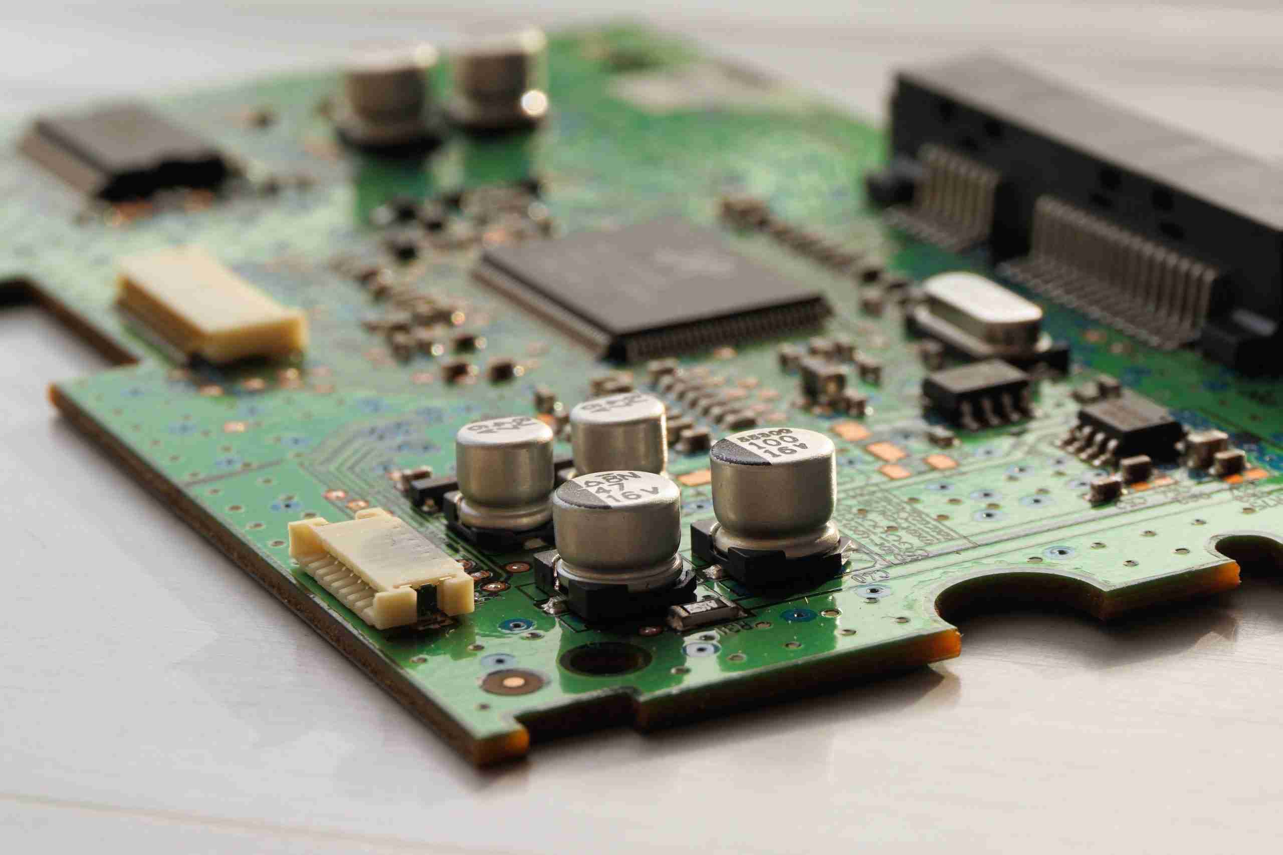
5. Through-Hole Component Addition and Soldering
For a few plans, not all components can be mounted utilizing surface mount innovation. Bigger components like connectors, transformers, or high-power transistors regularly require through-hole mounting, where component leads pass through gaps in the PCB. These components are either physically or naturally embedded into the PCB.
Once the components are in put, they are fastened utilizing wave fastening or specific patching strategies. In wave patching, the PCB is passed over a wave of liquid patch, which at the same time patches all the through-hole components.
6. Review and Quality Control
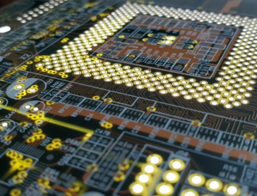
After soldering, the PCB undergoes a thorough inspection to ensure all components are correctly placed, and the solder joints are reliable. Automated Optical Inspection (AOI) machines use high-resolution cameras to inspect the PCB for defects like misaligned components, poor solder joints, or missing parts.
In a few cases, X-ray review is utilized to check for covered up surrenders, such as patch bridges or voids in Ball Grid Array (BGA) bundles. These assessments are basic to keeping up high-quality benchmarks in businesses like aviation or therapeutic gadgets, where indeed minor abandons can lead to failures.
7. Testing and Validation
Once the PCB assembly passes assessment, it experiences utilitarian testing to guarantee it works as expecting. Testing strategies can change depending on the complexity of the plan, but common procedures include:
• In-Circuit Testing (ICT): A strategy where each circuit on the PCB is tried separately to guarantee that all components are working correctly.
• Functional Testing: This strategy includes applying control to the PCB and confirming that the gathered board performs its planning work inside the bigger system.
• Burn-In Testing: In high-reliability applications like aviation, PCBs are subjected to amplified periods of operation at tall temperatures to guarantee they can handle push and won’t come up short prematurely.
8. Last Assembly
After testing, the PCBA may experience extra steps, such as including connectors, mounting it into a lodging, or connecting cables. The wrapped up item is presently prepared to be coordinates into the last gadget or system.
Surface Mount Technology (SMT) vs. Through-Hole Technology (THT)
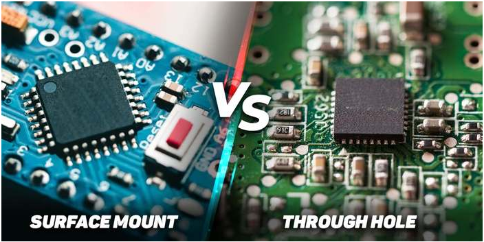
In PCB assembly, two essential strategies are utilized to mount components: Surface Mount Technology (SMT) and Through-Hole Technology (THT). Each strategy has its points of interest and is utilized depending on the particular application.
• Surface Mount Technology (SMT): In SMT, components are mounted specifically onto the surface of the PCB. This strategy permits for more compact plans and higher component densities, making it perfect for cutting edge hardware like smartphones, computers, and wearables. SMT is profoundly computerized, making it cost-effective for large-scale production.
• Through-Hole Technology (THT): In THT, components have leads that pass through gaps in the PCB, which are at that point fastened on the inverse side. Whereas THT is less compact than SMT, it gives more strong mechanical associations, making it appropriate for components that may involvement mechanical stretch, such as connectors, switches, and control components.
Advantages of PCB Assembly
PCBA offers a few focal points that make it the favoured strategy for fabricating electronic devices:
• Compact Estimate: PCBs permit for high-density plans, meaning more usefulness can be stuffed into littler spaces. This is fundamental for cutting edge electronic gadgets that prioritize compactness and miniaturization.
• Consistency and Unwavering quality: Mechanized PCB assembly forms guarantee that components are put and fastened with tall exactness, driving to reliable and solid performance.
• Cost-Effective: PCBs reduce the need for complex wiring and manual labor, lowering manufacturing costs, especially in large production runs.
• Durability: The materials utilized in PCBs, such as fiberglass and epoxy, are exceedingly tough and safe to warm, dampness, and chemicals. This makes PCBs perfect for cruel environments.
• Easy Investigating: The standardized format of PCBs makes it simpler to troubleshoot and repair issues. Engineers can follow issues to particular components or associations on the board.
Applications of PCBA Circuit Boards
PCBA circuit sheets are omnipresent in the cutting edge world, finding applications in a wide run of industries:
1. Consumer Gadgets: From smartphones to portable workstations to domestic apparatuses, about each electronic gadget we utilize day by day depends on PCBA circuit sheets for their functionality.
2. Automotive Industry: PCBA is utilized in car frameworks, engine control units (ECUs), infotainment frameworks advanced driver-assistance systems (ADAS), and more.
3. Medical Gadgets: Life-saving therapeutic gear such as pacemakers, imaging gadgets, and symptomatic machines depend on high-precision PCBA to work reliably.
4. Aerospace and Defense: The aviation and defense businesses utilize PCBA in flying, radar frameworks, communication gear, and other basic frameworks. These businesses require exceedingly dependable and vigorous PCB congregations due to the cruel situations in which the hardware operates.
5. Telecommunications: PCBA circuit sheets are fundamentally to broadcast communications foundation, empowering the working of switches, switches, base stations, and portable devices.
Challenges in PCB Board Assembly
While PCBA has revolutionized hardware fabricating, it does come with certain challenges:
• Miniaturization: As gadgets ended up littler, the request for more compact PCBs with higher component densities increments. This can make challenges in terms of component situation and fastening, as there is less room for error.
• Thermal Administration: With more components pressed onto littler sheets, warm dissemination gets to be a basic concern. Disappointment to oversee warm viably can lead to untimely component failure.
• Component Accessibility: The worldwide hardware supply chain can be unstable, and deficiencies of key components can disturb the assembly process. Producers must be dexterous and have possibility plans in place.
• Testing Complexity: As PCBs ended up more complex, testing gets to be more challenging. Guaranteeing that all components and circuits work accurately requires advanced testing strategies and equipment.
Future Patterns in PCB Assembly
The future of PCB assembly is shinning, with a few energizing patterns balanced to reshape the industry:
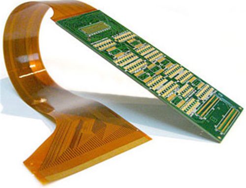
• Flexible and Rigid-Flex PCBs: Adaptable PCBs, made from materials like polyimide, permit for more flexible plans, particularly in wearable gadgets and therapeutic gadgets. Rigid-flex PCBs, which combine both inflexible and adaptable layers, offer the best of both universes in terms of strength and flexibility.
• Miniaturization and High-Density Interconnect (HDI) Innovation: As electronic gadgets proceed to shrivel, the request for miniaturized PCBs with higher component densities will increment. HDI innovation, which employments microvias and lean layers, permits for more compact plans without relinquishing functionality.
• 3D Printing and Added substance Fabricating: 3D printing innovation is making advances into PCB fabricating, advertising the potential to make complex, multi-layered PCBs rapidly and cost-effectively. This could revolutionize prototyping and small-batch production.
• Environmentally Inviting Fabricating: As concerns approximately the natural affect of hardware fabricating develop, there is expanding intrigued in utilizing eco-friendly materials and forms in PCB assembly. This incorporates lead-free patch, biodegradable materials, and more energy-efficient fabricating techniques.
Conclusion
Printed Circuit Board Assembly (PCBA) is the spine of advanced hardware, empowering the creation of gadgets that control our world. From customer hardware to aviation frameworks, PCBA plays a crucial part in guaranteeing that electronic frameworks work dependably and efficiently.
As technology continues to evolve, so too will the methods and materials used in PCB board assembly. Miniaturization, flexible PCBs, and 3D printing are just a few of the trends that promise to shape the future of this critical industry. Regardless of these changes, the importance of high-quality PCBA will remain constant, ensuring that our devices continue to function flawlessly in an increasingly connected world.
Latest Blog

Contact Info
Phone: +86-755-82882936
Email: [email protected]
WhatsApp: +86-13570802455
Wechat: +86-13570802455
Address: 2nd floor,D Bldg.,Electric Link Technology Bldg.,Gongming,Guangming New Dist.,518106 Shenzhen, China