Process Control of Key SMT Procedures–Patch
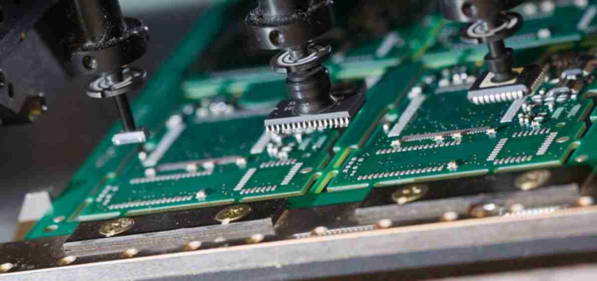
Table of Conent
Table of Conent
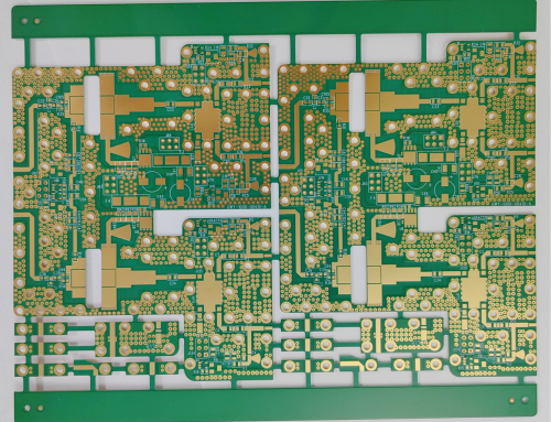
The core processes of SMT processing include solder paste printing, SMT machine operation, and reflow soldering. Only by effectively controlling the SMT process flow can we ensure the excellence of processing quality and improve efficiency.
First. Understand the principle of SMT machines and improve the quality of SMT
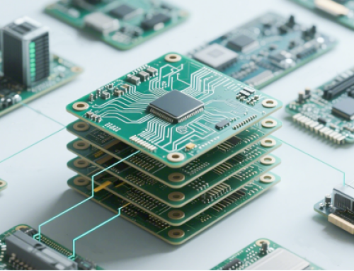
As key equipment in the SMT production process, the SMT machine is a precision industrial automation robot that integrates electromechanical, optical, and computer control technology. Based on the guidance of the SMT program, the equipment uses the vacuum suction, displacement, positioning, and placement functions of the suction nozzle through the cooperation of the feeder or tray. Under the premise of not damaging the components and printed circuit boards, it can quickly and accurately mount SMC&SMD components to the specified pad position of the PCB.
1. PCB calibration principle of SMT machine
When the SMT machine performs the mounting operation, the coordinates and angles of the components are usually based on a specific corner point (usually the lower left corner) on the printed circuit board (PCB) as the reference origin. However, in the process of PCB positioning, there will inevitably be a certain deviation.
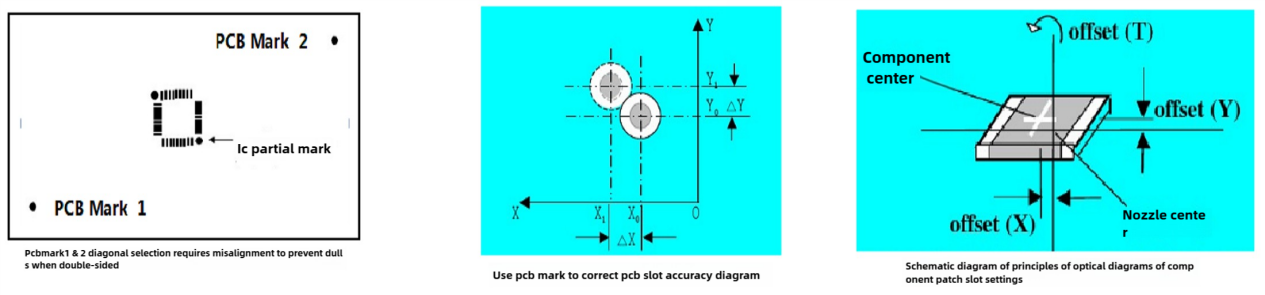
Therefore, before the mounting operation begins, the position of the PCB must be accurately calibrated. Usually, the reference mark (also called mark point) on the PCB is used to compare and calibrate the optical system of the placement machine. For precision components, such as QFP/BGA, in addition to using PCB Mark points, the local Mark points of the element itself are also used to further accurately correct the potential errors of PCB positioning to ensure the quality of the placement operation.
2. The centering method and principle of the components picked up by the SMT machine
Before the components are picked up and mounted, the feeder (or tray) must be centered because deviations may occur during the feeding and vacuum nozzle absorption. There are usually three principles of centering: mechanical centering (correction by applying external force through mechanical centering claws), laser centering (centering by optical projection, correction during the SMT process, and discarding if correction is not possible), and visual centering (comparing the components in the program library with CCD cameras, correction during the SMT process, and discarding if correction is not possible). All three methods can screen abnormal components, such as deformed pins and inconsistent thickness, and throw abnormal parts into the recycling box.
Second. Three elements to ensure the quality of SMT
1. Correct use of components
The basic characteristic identification of each mounting position number component, such as material model, package, nominal value, and polarity, must be consistent with the requirements of the product’s BOM, PCB surface and position number, angle, and other engineering data. The brand restrictions of the material manufacturer specified by the customer must also be strictly followed to ensure accuracy.
Assypcb is committed to working closely with high-quality suppliers. On the one hand, it continues to expand the types and brands of supplied materials, establish a basic material database, and adopt a material tracking and identification barcode (S/N) system. On the other hand, Assypcb continues to optimize the functions of the intelligent identification and matching system, encodes and identifies the materials provided by customers, and combines them with the material tracking and identification barcode (S/N) system. In addition, through the intelligent platform, the patch machine line and machine number, patch program, etc. are integrated to form a unique function of the error-proofing system, aiming to achieve error-proofing in the production process and trace the material information on the PCBA afterward, and provide registered customers with effective quality monitoring, traceability means and data support.
2. Accurate component placement position
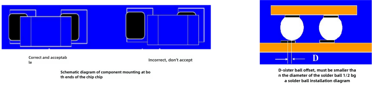
The terminals or pins of the components should be accurately aligned and centered with the pad pattern, and ensure that the welding end of the component has good contact with the solder paste pattern. For CHIP components with two terminals, the self-positioning effect is more significant. Therefore, during the mounting process, more than three-quarters of the length in the width direction should be covered on the pad, and the two terminals in the length direction only need to overlap the corresponding pad and contact the printed solder paste pattern. During the reflow soldering process, the components will be naturally aligned. However, if one of the terminals fails to overlap the solder paste pattern or pad, reflow soldering may cause component displacement, tombstones, or indirectly cause defects such as solder beads.
For BGA component mounting, the solder ball should be accurately aligned with the corresponding pad, and the maximum offset between the center of the solder ball and the center of the pad should be less than half of the solder ball diameter. This is the basic principle for soldering alignment.
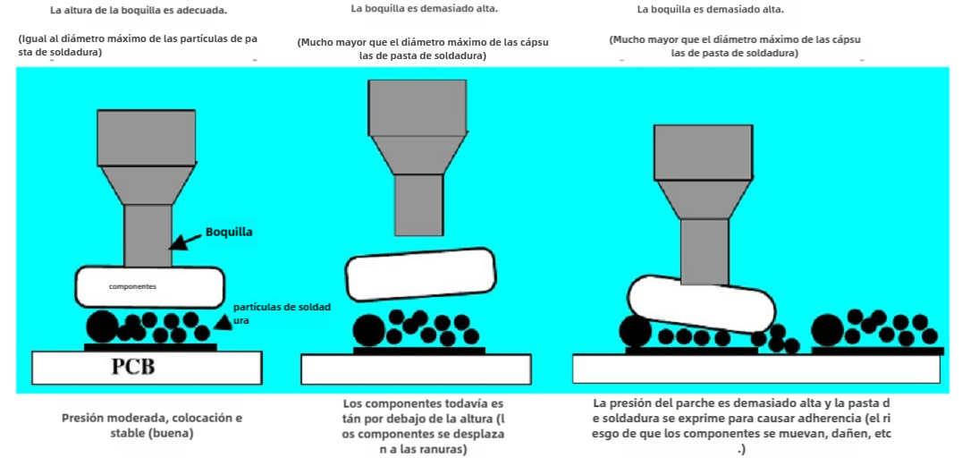
3. The nozzle pressure (patch height) is moderate
The nozzle pressure (i.e. patch height) is set mainly based on the component package height, the feeder/tray feeding plane, and the Z-axis height of the nozzle. If the patch pressure is insufficient, the component or its pin may float on the solder paste surface, resulting in the solder paste adhesion being unable to effectively fix the component, which is prone to positional displacement during the transmission and reflow soldering process. In addition, due to the excessive height of the X-axis, the component may fall from a higher position during patching, causing the patch position to shift. On the contrary, if the patch pressure is too high, the solder paste may be crushed and squeezed out too much, causing the solder paste to stick together, which is prone to bridge short circuits during reflow soldering; at the same time, due to the sliding effect, the patch position may also shift, which will aggravate the short circuit phenomenon, and in severe cases may even directly damage the component, resulting in difficult-to-detect internal or external damage, affecting the performance and reliability of the component.
Third. How to ensure the placement quality of the placement machine
1. Preparation and adjustment of the placement program
The accuracy and quality of the placement program have a decisive impact on the placement accuracy and efficiency. Therefore, it must be compiled based on the database independently developed by the Assypcb platform and combined with materials such as BOM/coordinate files. This is to ensure the correct coordinates and angles of each component position number on each face. At the same time, it is necessary to comprehensively consider the reduction in the number of nozzle changes, the minimization of placement head movement, the possibility of multiple placement heads sucking at the same time, and the avoidance of mutual interference and influence between the front and rear placement components, to optimize the PCBA component placement to achieve the best placement order and path. In the case of multiple machines in series production, the material types of each machine should be concentrated as much as possible, the advantages of each piece of equipment should be fully utilized, and the placement time should be as close as possible (in principle, the front process can be shortened by a few seconds) to maintain the optimal utilization of the production line capacity.
When the patch program is compiled and adjusted to the patch machine, special attention must be paid to the positioning of the PCB origin, the selection of the Mark point (including the foolproof measures for the order and direction of the board), and the compilation of the program (involving areas, size graphics, and contrast, etc.). These aspects are crucial to ensure the accuracy of PCB board entry and positioning; for precision devices such as QFP/QFN/BGA, local Mark points must also be set to improve the accuracy of device placement.
The name of the edited patch program generally needs to include information such as customer code-product model-patch machine brand-machine-side number, etc., to ensure that the program is completely matched with the engineering data such as the BOM to which the order belongs, and to ensure that the instructions are correct.
2. Preparation before placement
a. The “Order Information Sheet”, and “Material Loading Sheet” received before placement, the material identification of the feeder that has been prepared, and the consistency of the patch program are confirmed again.
b. Check whether the MSD moisture-sensitive components are effectively baked.
Before SMT PCBA processing, the MSD level of components such as PCB, BGA, QFP, QFN, etc. must be re-evaluated. When unpacking the components, check the included humidity indicator card to see if the 20% position has changed from pink to blue. If this happens, the component has been exposed to moisture and the baking procedure must be performed immediately.
The baking temperature and duration of MSD (moisture-sensitive device) should be considered comprehensively based on the level of MSD, the packaging method of the material, and other factors. Generally, for BGA, QFN, QFP and other packaging forms loaded on a 150°C tray and non-OSP (organic solderability protective film) treated PCB (printed circuit board), the baking temperature is set to 125°C±5°C and the duration is between 8 and 24 hours. For materials in reel packaging (paper tape and plastic tape), due to their relatively low-temperature resistance, the baking temperature should be controlled at 60°C±5°C and the duration ranges from 8 to 72 hours.
Please note that the baking time is not included in the time limit promised by Assypcb, the core principle of the baking process is to use a specific controllable temperature to gradually discharge moisture from the PCB/device to prevent the moisture inside the device from forming bubbles due to rapid temperature rise during the reflow soldering process, thereby affecting the electrical performance of the device (such as the internal welding lead of the device falling off, the package bursting, the PCB layer cracking and other potential quality risks). Therefore, customers are kindly requested to effectively seal the MSD devices provided and provide the necessary baking time throughout the manufacturing process to ensure the quality reliability, stability, and guarantee of PCBA processing.
c. Safety inspection must be carried out before starting the machine to ensure safe operation
The main inspection items include but are not limited to:
Whether the vacuum pressure of the equipment is above 6kg/cm2
Whether the rail width of all equipment and facilities is consistent with the PCB width
Whether there will be solder paste and mounting requirements on the moving part of the PCB rail
Whether the size of the PCB is greater than 50*50mm to ensure smooth transmission
Whether there are other debris or hanging objects affecting the PCB/PCBA transmission process
PCBA is effectively transmitted to avoid wiping off solder paste and components
FEEDER is firmly positioned and installed on the material table and buckled tightly without upward deformation
There are no obstacles in the nozzle movement route that may cause potential damage to the nozzle and mounting head
It can only be started when the mounting regulations are met.
3.First piece product
Personnel with specific operation certificates operate the first piece by the equipment’s operating procedures
4. IPQC first piece inspection
After the first piece of the order is produced, the technician will conduct a preliminary check on the mounted components based on the bill of materials (BOM), “Component Position Silk Screen Map” and “Material Loading Table”. The focus of the verification is to ensure that the device’s class number is correctly mounted, which includes but is not limited to the correct use of materials, polarity, and angle accuracy. At the same time, the accuracy of the mounting must be checked to ensure that the mounting position is correct, the pressure is appropriate, and there are no missing or incorrectly mounted components.
After the technician confirms that it is correct, the sample will be submitted to IPQC for process material testing. Assypcb is responsible for configuring a dedicated first-article inspection system, which can import the BOM, coordinate files, and component position silk screen provided by the customer, and automatically generate the first-article inspection program according to the established operating procedures. Under the guidance of the program, each CHIP-R/C/L component is clamped, and the system will automatically determine its correctness. The system automatically determines whether the component value is correct based on the nominal value and error range of the BOM material of the specified number. For other types of devices, manual comparison is used.
Since the first article inspection system has an automatic guidance function, it can complete the inspection quickly, and the inspection data can be automatically recorded by the system for subsequent reference, customers are kindly requested to ensure the integrity of the parameter information in the BOM (including but not limited to specifications, models, errors, etc.). At the same time, the coordinate file should be decomposed into front and back views, the silk screen of the component position should be clear, and the component position number and angle/polarity should be marked so that the system can efficiently perform inspections and pass the reflow oven process smoothly.
5. After the first piece inspection
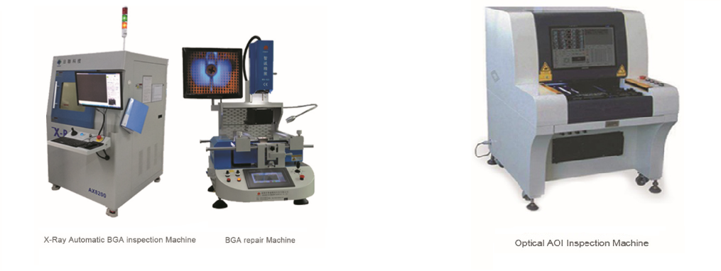
After the first piece inspection is correct, the PCBA will be soldered in the reflow soldering furnace at the appropriate spacing. If the PCBA contains BGA components, additional X-ray laser inspection is required to ensure that the BGA soldering position is accurate and no defects such as bubbles. If problems are found during the inspection, they should be recorded in detail and reported to the technicians so that the causes can be analyzed and targeted measures can be taken (including but not limited to adjusting the program, isolating and correcting the mounted PCBA, etc.) until all products fully meet the standards before formal production can begin.
6. After the first piece inspection
After the first piece inspection is qualified and enters the normal production stage, the PCBA will be programmed and automatically inspected by the fully automatic optical inspection machine (AOI) according to the inspection requirements. For any abnormalities in the production process, the technicians will analyze and implement revisions and improvement measures in subsequent production to continuously improve product quality and pass rate.
7. During the formal production process
During the formal production process, the BGA mounting and soldering effects will be sampled and inspected regularly by the established process and process specifications. At the same time, ensure that the temperature curve of the reflow oven is inspected at least once per shift and audited to ensure its compliance.
Forth. The main factors affecting the quality of mounting – equipment precision
With the increasingly thin and small sizes of various finished products, to facilitate carrying and continuously reduce energy consumption to enhance endurance, the size of components on the product control core PCBA tends to be more refined accordingly. Ensuring the control of PCBA mounting quality not only depends on an excellent operation team and its process integration and control capabilities but also fully automatic and high-precision mounting equipment.
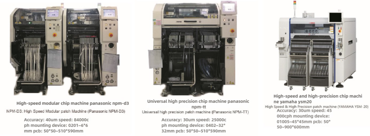
To meet the needs of registered customers in different industries for various PCBA processing, Assypcb has fully introduced high-speed and high-precision mounting machines imported from Japan that meet the high standards of the SMT industry. These include the Panasonic NPM-D3 model (showing the best performance in mounting SMC components), the NPM-TT model (showing the best performance in mounting SMD special-shaped devices), and the Elegant Maha YSM20 model (excellent in efficiently adapting to SMC/SMD versatility).
Latest Blog

Contact Info
Phone: +86-755-82882936
Email: [email protected]
WhatsApp: +86-13570802455
Wechat: +86-13570802455
Address: 2nd floor,D Bldg.,Electric Link Technology Bldg.,Gongming,Guangming New Dist.,518106 Shenzhen, China