The Future of Compact Electronics: Embedded Components on PCBs
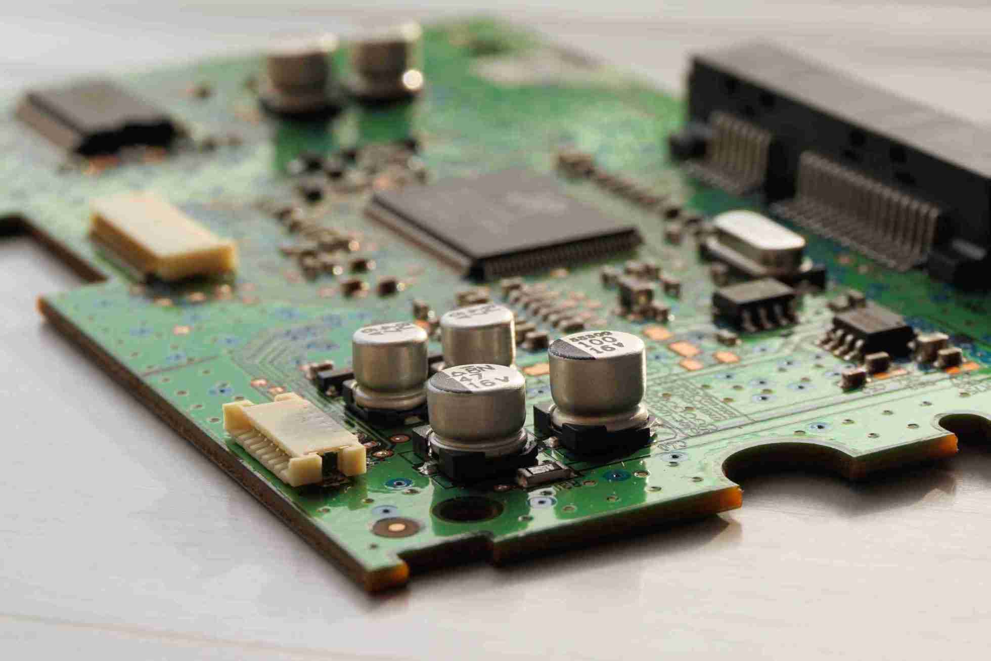
Table of Conent
Table of Conent
The conventional design and format of printed circuit boards(PCBs), as the demand for smaller and more productive electronic gadgets continues to grow, are being stretched to the limit. The increasing weight of electronic devices is driving the need for innovative arrangements. One of the most advanced concepts that will shape the future of compact hardware, is the integration embedded components into PCBs. Producers can produce more compact, efficient, and robust devices by implanting mechanical, inactive, or dynamic components directly into the PCB substrate.
This detailed article will explore the world embedded components on PCBs. We’ll look at how they function, what their challenges are, and the importance of their role in the advancement of the future of compact electronic.
What Is Embedded Components on PCBs?
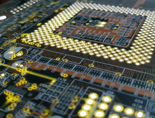
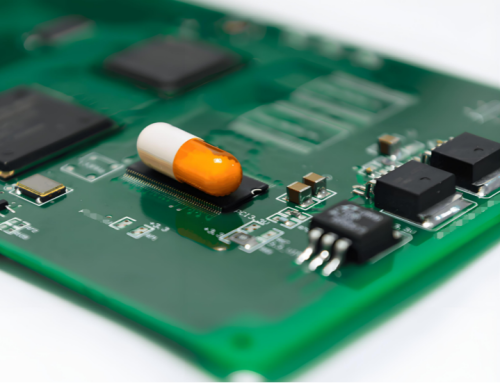
As opposed to components mounted on the surface, embedded components are positioned into specific layers of the PCB. Embedded components include both static components, such as transistors and diodes, as well as detached components, like resistors and capacitors.
The arrangement of the components within the layers is what makes a PCB with embedded components different from a conventional one. It allows for more compact designs and eliminates the need for additional surface-mounted components. The embedded components are placed inside the PCB using advanced manufacturing methods, ensuring perfect electrical connections and integration with other circuits.
Types of Embedded Components
The embedded components on PCBs are categorized into three main types.
1. Passive components: Resistors and capacitors that do not open up the signal.
2. Active Components (also called active components): These are gadgets like transistors, diodes and ICs which control electrical signals.
3. Mechanical Components: These components include sensors or switches which can be integrated to enhance the functionality of a device.
How Embedded Components Work
The process of inserting components into a PCB involves placing detached or dynamic components within the inner layers of the PCB during the creation procedure. The components can be inserted discretely or manufactured using other manufacturing techniques, such as thin film testimony. Electrical follows and vias on the PCB allow for consistent communication across layers.
Three key stages can be summarized:
1. Design stage: The layout and position of the components is decided during the planning stage. This includes the estimation, the warm distribution, and the necessary interconnections between layers.
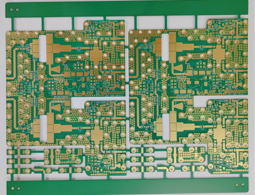
2. Manufacturing stage: During the creation of PCB, the embedded components are placed inside the PCB stack up some time after the last handle. The thin layers of copper foils and dielectric fabric are pressed together to form a multilayer PCB that contains the embedded components.
3. Testing and confirmation: A thorough test is conducted after manufacturing to ensure that all components are correctly inserted and connected.
The Advantages of Embedded Components in PCBs
1. Compact and Space-Efficient Design
Inserting components allows for smaller and more compact designs. By moving components to the interior of the PCB instead of the surface, designers can squeeze more functionality into a smaller impression. This is especially important in industries such as customer hardware where demand for compact gadgets such as smartphones, wearables and IoT devices is on the rise.
2. Enhancing Signal Integrity
Due to reduced parasitic capacitance and inductance, embedded components are more flag-aware. The components are embedded inside the PCB, closer to the signals that they supervise, so the flag paths are shorter. This leads to a lower resistance, and less misfortune with flags. This is essential for advanced circuits with high speeds and RF applications.
3. Upgrade Electrical Performance
The electrical performance of the PCB can be improved with embedded components. Near proximity of components to substrate reduces electromagnetic interference and noise. Warm dissemination has made great strides in recent years, allowing it to be easier to monitor warm issues within densely packed circuits.
4. Strength and Reliability Expanded
The embedded components are protected from external natural elements such as stickyness, neatness, and physical stretching. This increased security is achieved by a circuit that is more solid and durable, making it ideal for harsh environments such as aviation, automobiles, and mechanical electronic devices.
5. Manufacturing and Assembly Streamlined
The need for surface-mounted (SMD) devices is reduced by coordinating components within the PCB. This reorganizes the assembly handle. The less components that are on the surface, the fewer patch joints there will be. This will lead to a higher level of unwavering quality as well as lower manufacturing costs. The bill of materials will also be less complex.
6. Investment in High-Volume Production
Although the initial cost of developing implanted components can be high, it can result in a critical investment fund for high-volume production. By eliminating extra components and streamlining the gathering, it is possible to reduce the overall cost of producing huge quantities of PCBs.
Applications for Embedded Components on PCBs
The embedded component revolution is transforming different industries, resulting in the development of compact and high performance hardware. Below are some of the most important applications:
1. Consumer Electronics
As the demand for smaller, more energy-efficient, and capable gadgets grows, embedded component technology is quickly being adopted by consumer hardware such as smart phone, tablets, wearables and clever domestic gadgets. By embedding components in the PCB, manufacturers can create gadgets with greater functionality and efficiency.
2. Automotive Electronics
The demand for high-performance, compact hardware has increased as vehicles have become more autonomous and zapped. Installed components are able to help reduce the size and weight of electronic car frameworks while ensuring unwavering performance in harsh working conditions.
3. Aerospace and Defense
Aviation and defense industries require robust, durable gadgets that are able to withstand extreme situations. Embedded systems offer improved assurance and execution.
4. Medical Devices
The embedded components of implantable medical devices, like pacemakers and hearing aids, benefit from their miniaturization, and the unwavering quality they promote. This technology enables the development of smaller, more comfortable and longer lasting therapeutic devices.
5. IoT Devices and Smart Devices
Compact, low-power devices are needed to expand the IoT. These gadgets can be easily coordinated into various items and situations. Embedded elements help achieve these goals while enabling expanded functionality.
6. High-Performance Computing
In supercomputers and information centres, where space is limited and control ability is crucial, embedded components are a great way to improve performance while reducing the overall appearance of computer systems.
Manufacturing Techniques of Embedded Components
A number of manufacturing procedures were developed to facilitate the integration and use of embedded components on PCBs.
1. Laser Ablation
The laser removal technique is used to create precise cavities on the PCB layers, where components can be placed. This technique allows for precise positioning and measurement of embedded components.
2. Photoimageable Dielectrics
To create cavities and structures within the PCB layers, photoimageable dielectric material can be used. These materials can also be uncovered to create the desired designs and frames for implantation of components.
3. Additive Manufacturing
For PCBs that have embedded components, additive manufacturing strategies such as 3D-printing are being explored. This allows for greater plan adaptability as well as the possibility of customized, on-demand manufacturing.
4. Lamination Techniques
The PCB is bonded together using advanced cover forms, which are used to show the embedded components.
5. Direct Compose Technologies
Direct composition innovations such as inkjet and vaporized fly print are being developed to directly store conductive leads and even a few separated components onto the PCB substratum.
Future Patterns and Innovations
As the innovation of implanted components continues to progress, certain patterns and developments emerge:
1. 3D Printed Electronics
Combining 3D printing and implanted electronic components opens up previously unimagined possibilities for creating complex three-dimensional structures. The combination of implanted components and 3D printing innovations is opening up unused conceivable outcomes for making complex, three-dimensional electronic structures.
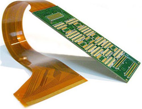
2. Flexible and Stretchable Electronics
The advancement of stretchable and bendable gadgets can be attributed to the embedding of components into adaptable substrates. This innovation can be used in wearable devices, delicate mechanical autonomy and similar sensors.
3. Integrating with Progressed Materials
Researchers are examining the integration of embedded materials with advanced materials, such as graphene or other 2D materials. This could lead to significant changes in functionality and execution.
4. Antennas Embedded
The embedded radio wires in PCBs will improve the performance and reduce the cost of remote gadgets. This is particularly important for IoT and 5G applications.
5. Power Hardware Integration
Inductors and Transformers are increasingly being embedded in control components, which allows for more compact and efficient control supply designs.
6. Artificial Insights & Machine Learning
As AI and machine-learning become more prevalent in electronic gadgets and devices, embedded components are going to play a crucial role in empowering edge computing capabilities that are more productive and capable.
Challenges for the Future
Although the future of embedded PCB components looks promising, a few challenges still need to be addressed.
1. Design Devices and Software
To fully utilize the potential of embedded elements, more advanced plan apparatuses are needed. These instruments should be able handle 3D planning and reproduce the execution of embedded frameworks with accuracy.
2. Materials Research
It is essential to continue investigating unused materials in order to improve the quality and manufacturing of embedded components. This includes creating better dielectric, conductive, and encapsulant materials.
3. Manufacturing Scalability
In order to meet the growing demand for innovative implanted components, it is necessary to make manufacturing processes more flexible and cost-effective. This could require a critical investment in equipment and processes that are unused.
4. Education and Training
Hardware industry must contribute to instruction and preparation to develop the skills required for PCBs that have embedded components.
5. Standardization Efforts
To ensure consistency and compatibility across diverse suppliers and producers, industry-wide guidelines must be developed for embedded component manufacturing and testing.
Conclusion
The inclusion of embedded components into PCBs is a significant step in the development of electronic design. By integrating components into the PCB, architects are able to create smaller, more efficient, and more durable electronic gadgets. This technology is making waves now in industries such as consumer hardware, automotive, aviation, and health gadgets.
There are many challenges in the development of any new innovation. These include plan complexity, manufacturing methods, and standardization. Nevertheless, the benefits of implanted component technology far outweigh these obstacles. The future of compact hardware is in the continued advancement and refinement implanted component technologies.
We can expect to see more innovative applications of implanted parts in the future. From adaptable and stretchable gadgets, to advanced 3D-printed structure. In the future, electronic devices will be driven by the integration of embedded technologies with other innovative innovations, such as 5G communication, fake insights and advanced materials.
It is vital that engineers, producers, and creators of gadgets stay on top of the latest advances in implanted components. The innovators who are able to successfully use this technology will be in a good position to create the innovative, compact and high-performance gadgets of tomorrow.
In conclusion, embedded PCB components are not a passing trend but an important move in the way we approach electronic design. As innovation continues to advance, it’ll play a more and more important role in shaping the future of compact gadgets. It will empower modern possible outcomes and push the limits of what is conceivable for electronic gadget design.
Latest Blog

Contact Info
Phone: +86-755-82882936
Email: [email protected]
WhatsApp: +86-13570802455
Wechat: +86-13570802455
Address: 2nd floor,D Bldg.,Electric Link Technology Bldg.,Gongming,Guangming New Dist.,518106 Shenzhen, China