The Initial Stage of PCB Manufacturing – PCB Layout Design
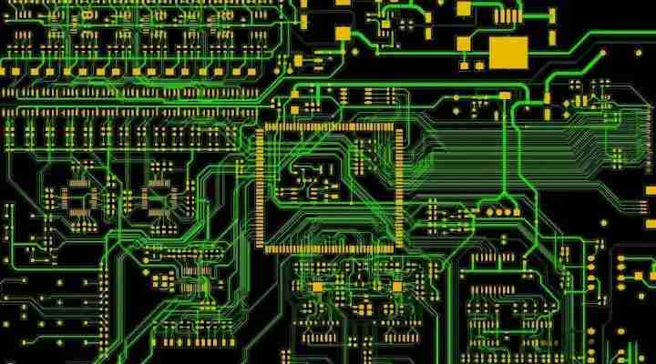
Table of Conent
Table of Conent
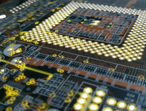
A printed circuit board‘s component arrangement and electrical connections are referred to as the assembled circuit board layout. In essence, it is a map that indicates the locations of each component and how electrical impulses go between them. In a word, the circuit board layout is the schematic used to build the real circuit board. It specifies the resistors, capacitors, integrated circuits, connections, and the routing of the copper traces that carry the current. The effectiveness of this layout creation determines the overall success of an electronic system. It guarantees proper component connections, effective electrical signal propagation, and that the finished product satisfies its performance and functional requirements.
How Can a PCB Layout Be Made?
1. Begin with the schematic design: A schematic is required before a circuit board can be laid out. The circuit’s components and their electrical connections are depicted in the diagram. The assembled circuit board layout is based on this concept, which directs wire routing and component placement.
2. Component placement: This stage necessitates giving component placement some thought. Components should be placed appropriately – important parts such as connectors or power supplies should be positioned to make wiring and assembly of the board easier. To reduce signal interference, high-frequency components should be positioned close to one another.
3. Routing Trace: An alignment is an electrical path that connects components. Creating pathways for signals to move between components is known as routing an alignment. To reduce resistance and signal latency, the alignment must be routed in the shortest way feasible. To prevent interference, extra care must be given while routing the alignment for sensitive signals or high-power components.
4. Describe the ground and power planes: Large sections of copper make up the power and ground layers, which give components a steady voltage reference. These layers help reduce noise and improve circuit stability. In high-speed or high-power circuits, proper grounding is especially crucial to prevent interference and voltage swings.
5. Take thermal management into account: Heat produced by power-consuming components might lead to issues if improperly controlled. To guarantee efficient heat dissipation, thermal vias, bigger copper surfaces, and heat sinks are occasionally needed. Thermal components can also be positioned away from high-power components to prevent overheating.
6. Execute a Design Rule Check: Following component placement and route alignments, you must review the design for mistakes. Potential issues such as alignment width violations, inadequate spacing, or incorrect component placement can be found with the use of an automated check called the Design Rule Check. To avoid overheating, thermal components can also be placed apart from high-power components.
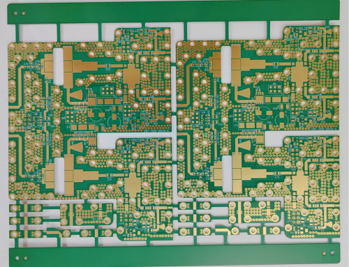
7. Finalize Layout and Export File: The design is prepared for production after the layout is finished and any issues have been fixed. Exporting the design file, often in Gerber format—the format required to make the actual assembled electronic board—is the last step.
What Is the Standard PCB Format?
1. The Gerber file, which lists the layers, alignments, holes, and components on an assembled circuit board, is the most popular format. To turn a layout into a real board, these files are necessary.
2. The Pick and Place Files show exactly where the parts need to be on the circuit board to finish the assembly process.
3. The Bill of Materials is a list of all the parts needed for the circuit board, including the part numbers, quantities, and other important information.
Every format has a distinct function in guaranteeing that the design may be precisely produced and put together.
How Long Does the PCB Layout Take?
The complexity, number of layers, and level of competence of the designer all affect how long it takes to create an assembled circuit board layout. It could take weeks or months to complete complex designs, such as those with several layers or high-speed components. The timeline may be impacted by the project’s complexity, the requirement for iterative testing, and the degree of optimization. The more layers and components in the design, the longer it takes to finish the layout.
What Makes PCB Layout Crucial?
1. A well-designed electronic card layout makes sure that electrical components work properly. If you have improper wiring or arrangement, your device might break down.
2. You can reduce power loss and improve your circuit’s efficiency by choosing the right trace widths and optimizing trace lengths.
3. Properly routed lines improve signal integrity and reduce electromagnetic interference. In applications involving high speed or radio frequency , this is particularly crucial.
4. Prevent Overheating: An essential component of printed circuit card layout is efficient thermal management. Wide copper alignments, heat vias, and heat sinks are all important in preventing component overheating, which can fail.
5. Enhance manufacturing ability: A well-thought-out printed circuit card layout that complies with industry standards makes board manufacturing simpler and more affordable. Following the right layout guidelines guarantees that boards are made more cheaply and with fewer mistakes.
6. Future upgrade support: It’s simpler to alter and enhance your design in the future when electronic card layouts are clear and thoroughly documented. Whether you need to add a new feature or solve an existing problem, a good layout helps make the process easier.
How Can My PCB Layout Be Made Better?
1. Maximize your circuit board layout: Reduce the length of the trace: Resistance, noise, and delay are all decreased with shorter alignments. Particularly for high-frequency or high-power components, make an effort to keep traces as straightforward as possible.
2. Use wider spacing for components that use a lot of electricity. For components that use a lot of power, use wider spacing or special wiring to prevent overheating and power loss.
3. Avoid crossing traces. These alignments can make your design more complex and lead to errors. By carefully arranging the components, try to prevent needless crossings.
4. Group components that are related. Assemble components that collaborate closely to reduce the requirement for lengthy connections. This enhances signal quality and simplifies cabling.
5. Make use of power and ground layers: A strong ground and power layer lowers noise and helps maintain a steady voltage. Particularly with high-speed designs, this is crucial.
6. Look for any infractions of the design rule: You may ensure that your layout conforms with manufacturing specifications and industry standards by using automated design rule checks. These checks aid in preventing mistakes that can make production more difficult.
7. Consider heat management as well. Pay attention to components that conduct heat and how close they are to components that use a lot of power. Include heat vias or large copper areas for effective heat dissipation.
What Guidelines Govern the Design of Printed Circuit Board?
Certain guidelines are essential for developing a circuit board layout to produce a board that is both functional and able to be manufactured. Among the key printed card circuit designing guidelines are alignment width and spacing:
1. alignment width and spacing: Verify that the alignments are sufficiently far enough to avoid short circuits and that they are broad enough to support the current they can manage.
2. Placement of Components: Components should be arranged with minimal trace lengths and clear signal routes. To reduce signal attenuation, high-speed components should be positioned near one another.
3. Signal Integrity: To prevent noise or interference, keep high-speed signal traces as short as feasible and do not run parallel to power supply wires.
4. Thermal management: Thermal management involves putting thermal components away from power components and adding heat sinks or thermal vias as necessary.
5. Grounding: To minimize noise and provide the circuit with a steady reference, always incorporate a solid ground plane.
What Distinguishes PCB Design from PCB Layout?
Despite their frequent interchangeability, the words “PCB layout” and “PCB design” really refer to two distinct stages of the PCB production process.
• PCB design is the general planning phase, which includes creating schematics, choosing components, and organizing the circuit’s overall functioning.
• PCB layout is all about arranging the parts and planning the connections. It’s like making a map.
Conclusion
The effective functioning of every electrical circuit depends on a carefully thought-out PCB layout. It guarantees effective signal flow, reduces power loss, and enhances the device’s overall dependability. For the finest solution, get in touch with us if you require a PCB design layout.
Latest Blog

Contact Info
Phone: +86-755-82882936
Email: [email protected]
WhatsApp: +86-13570802455
Wechat: +86-13570802455
Address: 2nd floor,D Bldg.,Electric Link Technology Bldg.,Gongming,Guangming New Dist.,518106 Shenzhen, China