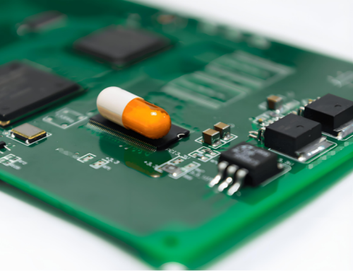
What Are the Methods and Precautions to Prevent PCB Deformation?
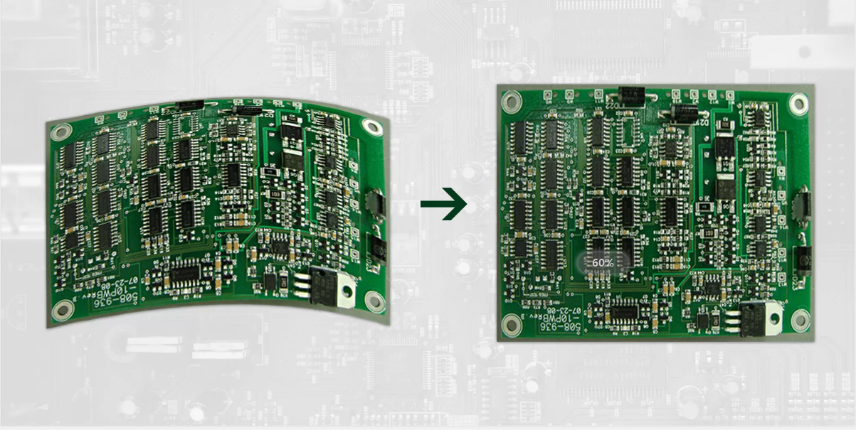
Table of Conent
Table of Conent
PCB bending or warping can cause a host of problems. If you’re lucky, the effects of the warping may be so minor that you don’t even notice it. On the other hand, it may be so severe that it can cause immediate electrical problems.
Warping is often a result of reflow welding. In severe cases, it can even cause components to stand up and result in empty welding situations. Warping can also be caused by thermal mismatch, as different materials experience thermal expansion at different rates.
reasons for warping and bowing
Although there can be many reasons for warping and bowing, the main one is caused by high stress on the board. This can be due to the following reasons:
1. Copper surface area – When the area of the copper surface is uneven, it causes uneven heating and cooling, which can cause deformation.
2. Weight of the board – The weight of the board itself can cause sagging
3. V-cuts – The depth of the V-cuts and the way they are connected can cause deformation
4. Connection points – Vias on each layer restrict the expansion and contraction of the board.
Methods to ensure no warping occurs
According to IPC-6012, the maximum allowable package thickness for PCB surface mounting is 0.75%. Therefore, it is important to find effective ways to ensure that warping does not occur. Here are some:
Lower the temperature
Due to the temperature, a lot of stress is generated on the board. Therefore, it is necessary to lower the temperature of the furnace or adjust the rate at which the temperature is increased, and adjust the subsequent cooling.
High Tg
The transition temperature of glass, which is the temperature at which glass changes its state, affects warpage. The lower the Tg value of a material, the more severe the deformation may be. Therefore, even if the material cost is higher, a sheet with a higher Tg can improve its ability to withstand stress.
Board thickness
The thinness of electronic products required these days affects the circuit board and often causes deformation after passing through the reflow oven. If the thickness can be kept at 1.6mm, the possibility of board deformation can be significantly reduced.
Number and quantity of boards
Most reflow ovens use chains. Therefore, large-sized boards may deform in the oven due to their weight. So, it is recommended to use the long side of the board as the board edge.
Oven tray
Using an oven tray can also reduce deformation. If a single tray cannot reduce deformation, adding a lid can also solve the problem.
Symmetrical arrangement
Semi-cured sheets should be arranged symmetrically. Otherwise, they may warp. For example, in an 8-layer board, the thickness and quantity of prepreg should be the same in 1~2L and 7~8L. Otherwise, the board may bend. It is also subject to use products from the same supplier for multi-layer and semi-cured boards.
Longitude and Latitude of Prepreg
The warp and weft shrinkage of the prepreg after lamination is different. It is best to roll the prepreg in the longitude direction and the width in the latitude direction.
Decompression after lamination
After hot and cold pressing, the laminate needs to be taken out and laid flat in the oven to release the stress on the board. Baking the laminate at 150 degrees Celsius for about 8 hours can remove excess water and solidify the resin.
Flat Straightening
When using thin multi-layer boards for surface and pattern plating, it is important to use special clamping rollers. Once the board is clamped on the plating line, the clamping rollers need to be tightened so that all boards are straightened. If this process is missed, the board may bend, and the deformation may be difficult to correct.
Cooling the board after hot air leveling
The printed board must withstand the high temperature of the solder tank. It must be placed on a flat marble or steel plate to allow time for natural cooling.
Wood Board Processing
Shenzhen Assypcb SMT: Check the flatness of all PCBs. The uncut board is placed in an oven for 3-6 hours at 150 degrees Celsius and pressure. Due to this anti-warping process, sometimes part of the board can be saved.
Latest Blog

Contact Info
Phone: +86-755-82882936
Email: [email protected]
WhatsApp: +86-13570802455
Wechat: +86-13570802455
Address: 2nd floor,D Bldg.,Electric Link Technology Bldg.,Gongming,Guangming New Dist.,518106 Shenzhen, China