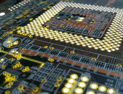
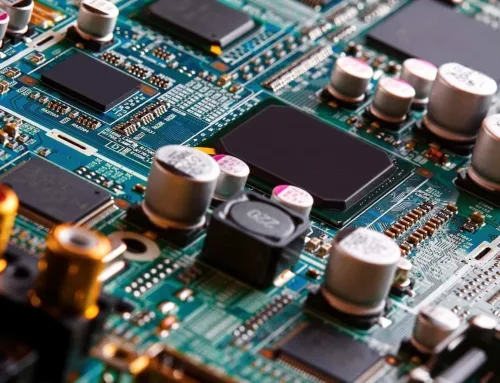
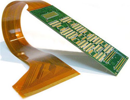
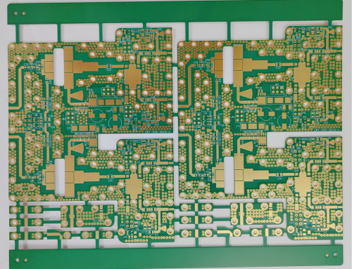
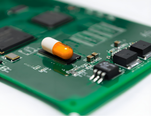
What Is PCB Nickel Plating?
Table of Conent
Table of Conent
The PCB finish Nickel, also known as electrolytique soudabilite, improves solderability and protects copper surfaces. Nickel is used as a base to prevent corrosion for further surface treatments. Electrolytic finishes such as gold or tin are then applied on top to increase conductivity and durability. They also make soldering easier. These finishes minimize oxidation and provide component connections that are reliable. These finishes also enhance PCB performance over time in a variety of environments. The application requirements are taken into consideration when choosing between nickel or electrolytic finishes. These include mechanical stability, electrical performance and thermal resistance.
Applying a nickel or electrolytic finish to a printed circuit board (PCB) is an important process that improves its ability to be soldered and protects exposed copper areas. Typically, a nickel undercoat is first durable and corrosion-resistant base, which is then covered with an electrolytic coating like gold or tin plating. This additional coating enhances conductivity, prolongs the lifespan of the PCB, and ensures secure bonding of components during soldering. By reducing oxidation and supporting the PCB’s functionality in various environments, the choice between a nickel or electrolytic finish depends on factors such as thermal resistance, electrical performance, and mechanical strength required for the specific application.
The Use of Nickel (Ni) Plating on PCB Boards
The application of nickel coatings on printed circuit boards (PCBs) leverages the unique properties of this metal. With its distinctive symbol Ni of industrial and engineering uses due to its outstanding attributes, including remarkable strength, corrosion resistance, and magnetic capabilities. The blending of nickel with metals such as steel, chromium, and copper results in the creation of strong and durable alloy materials. Additionally, nickel’s natural ability to withstand corrosion has historically made it a popular choice for minting coins.
What is meant by good nickel oxidation resistance? A special explanation is needed here. In fact, the activity of “nickel” itself to “oxygen” is quite high, that is to say, “nickel” itself can be oxidized easily, but due to the excellent fineness of the oxides (NiO, Ni(OH)2), a film is formed to cover itself, so that the oxidized nickel can be oxidized. However, due to the excellent fineness of the oxides (NiO, Ni(OH)2), they can form a thin film to cover themselves and insulate themselves from the air, and thus resist oxidation, which means that nickel oxidizes itself to form a protective film before being able to protect itself, and the base metal continues to oxidize from the jade.
This means that the nickel will oxidize itself to form a protective film before it can protect itself, while the base metal continues to oxidize from the jade. Therefore, “nickel” is often used in plating on other metal surfaces to protect the base metal from coming into contact with the air and causing oxidation. However, the plating layer must be “defect-free”. To a certain degree of protection, in the early nickel plating process, due to the process is not very mature, there are often small holes, so that the plating layer under the base metal material can not be completely sealed, resulting in oxidation of the base metal after nickel plating. Problems, and the current PCB nickel plating process has become increasingly mature, usually added to the plating tank sealer to solve the problem of air holes.
What Is the Purpose PCB Nickel Plating For?
Nickel plating PCBs serves several purposes. These include improving wear resistance, preventing metal diffusion, increasing mechanical strengths, and meeting the requirements of hot press brazing or soldering.
Nickel plating PCBs (Printed Circuit Boards) increases the wear resistance of switch contacts, contacts, and plug gold. Nickel acts as a barrier to prevent copper and other metals from diffusing. Performance and service lifetime.
The nickel layer enhances the mechanical properties of the gold surface and makes it suitable for use as a protective coat on precious metals or base materials.
• Nickel plating is a way to increase the corrosion resistance and protect a board’s surface.The circuit board can then be used in harsh environments.
• Nickel plating increases the resistivity of circuit boards, which improves signal transmission.
• Nickel plating improves the solderability by making the board easier to handle.
• Nickel plating is a good signal transmitting material. It is electrically conductive, reducing the loss of signals.
• Nickel plating improves mechanical strength and durability and increases the service life of the board.
How Thick Is PCB Nickel-Plated?
The PCB nickel layer is usually 22.5mm thick. Nickel is used primarily to protect and adhere gold or other precious materials. The thickness of the nickel layer has a major impact on the final product’s quality and appearance. A nickel layer of around 5 mm is sufficient.
PCB Nickel Plate Calculation Formula
The formula for calculating the thickness of PCB nickel plating is: The thickness of the plated layer is equal to: current density (ASF), plating time (minutes), and Plating efficiency (%) multiplied with 0.01821.
Formula description:
• Current density (ASF): Amperes/square feet per unit area
• Plating time (minutes): The amount of time needed to plate in minutes.
• Plating efficiency (%): This usually ranges between 90 and 100 percent.
• 0.0182: the current density, plating speed and efficiency. The plating factor converts current density and plating speed into thickness.
Calculate the nickel-plating thickness using an ASF of 10 and a 30-minute plating time.
Current Density: 10 ASF
Time to Plate: 30 Minutes
Plate efficiency: 95% (0.95
Factor of plating: 0.0182
Coating thickness = 10x30x0.95×0.0182=5.274microns
What Is the Difference in PCB Nickel Plating vs Tin Spraying?
1. Process Principle
The process of nickel plating involves applying a thin layer of metallic nickel to a circuit board through electrochemical deposition, which enhances its resistance to corrosion and improves its soldering capabilities.
Tin Spraying Tin spraying is also called thermal spraying and involves spraying a thin layer of tin on the surface. Tin spraying improves solder reliability, and protects circuit board corrosion.
2. Application Effect
Application Effect Nickel plating: The surface of the nickel-plated board has a uniform sheen. The nickel layer is tightly bonded to the substrate, preventing erosion from external environments. The nickel layer has a ductile, tough surface that is suitable for further processing and assembly.
Tin spray effect: A dense layer of tin-alloy is applied to the surface of the board, providing good electrical conductivity. The tin alloy is also resistant to corrosion. Tin spraying can be tailored to the specific requirements of an application.
3. Nickel Application Scenarios
Nickel is applied to higher circuit boards, such as those used in automotive electronics, communication equipment and other fields, in order to provide conductivity, corrosion resistance and good soldering. Nickel plating can be used to repair circuit boards, reinforce them or even enhance them.
Spray tin scenarios. Spray tin is best suited for circuit boards that have high requirements. These include those found in household appliances, industrial controls systems, and many other applications. Spray tin can be used for circuit board surface decoration as well as soldering reliability.
PCB Nickel Plating Uses Nickel Sulfamate
• Nickel sulfamate can improve plating efficiency by improving the speed of plating, promoting plating reaction and reducing plating times.
• Improved plating quality. Nickel sulfamate prevents crystallization, making nickel particles smaller and uniform. This produces a thicker and more uniform nickel layer.
• Nickel sulfamate is a stress-relieving agent. It is essential for plating complex-shaped items, as it prevents cracking or flaking.
• Control pH of plating Solution: Nickel sulfamate can maintain the pH in the plating solution, which is essential for maintaining consistency of plating quality.
How to Solder Nickel-Plated Pins onto PCB?
• Preparing the pads before soldering. Use a soldering iron to apply flux and avoid poor soldering due to oxidized pads or those that are not properly tinned. Placing the PQFP chip on the PCB using tweezers is the best way to do it. Check that the pins and the orientation of the chip are in alignment.
• Soldering a chip: Set the soldering temperature to 300 degrees Celsius. Dip a tip of an iron in a small amount of solder and press the chip with a tool. Solder the two pins in a diagonal direction to secure the chip. When soldering to prevent overlapping and overlapped soldering, make sure that the tip is parallel with all pins.
• Check and adjust: Use flux to remove excess solder after soldering the pins. Vacuum away any surplus solder to avoid overlaps or shorts. When checking for soldering mistakes, tweezers can be a useful tool.
Soldering Notes
• It is crucial to maintain a constant temperature in order to avoid poor soldering due either too high or too low temperatures.
• Handling pins incorrectly can cause weak soldering.
• Common problems and their solutions
• Pad Oxidation: If the pads are oxidized, they will lead to poor soldering. Before soldering, you can treat the pads with flux or other treatments.
• Damaged pins – Use tweezers carefully to avoid damaging pins.
Nickel-Gold Plating PCB
• To prepare the board for this process thoroughly clean the PCB to remove dirt and grease, ensuring the coating adheres properly, followed by a water rinse to eliminate any remaining degreaser residue.
• Next, a neutralizing agent is applied to restore the PCB’s pH balance, after which it is washed again to remove any residual agents.
• Next, a neutralizing agent is applied to restore the PCB’s pH balance, after which it is washed again to remove any residual agents.
• Immerse the PCB in pre-soak solution to prepare its surface.
• To improve the adhesion of the coating, the PCB surface is treated with an activating palladium solution.
• This water cleaning method uses blowing to clean the surface.
• Deposits a layer of electroless nickel onto the surface PCB.
• After electroless plating the electroless nickel is removed by a hot water wash.
• The final layer of gold is formed by a layer of chemically deposited gold on top of the nickel layer.
• After chemical deposition of gold, the solution will be removed with a recirculating rinse.
• This rinse is used to confirm that the surface was cleaned.
• Drying completes the nickel-gold plating.
A printed-circuit board can be given a PCB finish that is nickel or has an electrolytique effect. A nickel finish can be applied to a printed circuit board, which can be further enhanced with an electrolytic coating, such as gold, to improve both its appearance and functionality. This results in a sparkling effect similar to champagne. Functional benefits such as improved solderability, corrosion resistance and increased electrical conductivity enhance the aesthetic appeal.
This finish is used for luxury electronic products or high-end electronic applications where both performance and appearance are important. This finish is both durable and elegant.
PCB Nickel Adhesion Criteria National Standards
Standard GB/T 9286-298 is the standard for nickel plating adhesion testing. The test methods include the scratch test, impact and peel tests. You can choose the test method based on material characteristics and requirements.
Test Methods
• Test for cross-shaded line: Cut 10 x 10 small grids measuring one mm by one mm on the nickel plating. Each scratch line should be at least the same depth as the base layer of plating. Apply an adhesive tape after cleaning the area using a soft-bristle brush. 3M No. The tape’s adhesive strength should be between 350g/cm2 and 400g/cm2. After wiping the tape vigorously, remove it quickly and vertically. Peel-off condition.
• Peel Test: Peel off the nickel-plated sample to see if it flakes or has been deformed.
• Impact test the nickel-plated layer to determine its impact resistance.
Judgement Criteria
• 5B: The lines are smooth at the edges and intersections.
• 4B: It is defined as a small flake at the intersections between the lines scribed. This flaking has a surface area of less than 5 %.
• 3B: Small flake of coating at the intersections or edges of scribed lines with a flaking surface of between 5% and 15%.
• 2B: A flaking coating is present at the intersections of the scribed lines and the edges, with a flaking area ranging between 15 to 35 percent.
• 1B: Pieces of flaking coating at the edges or intersections between the lines scribed. The flaking area is between 35 to 65 percent.
• 0B: The overall flaking area exceeds 65%.
PCB Nickel Plating: Common Problems and Their Solutions
• Surface treatment is required before nickel plating circuit boards. This will guarantee that the board’s roughness and finish satisfy the specifications.
• It is important to know the formula for the molecular electrolytique in order to get the best nickel plating. The formula and concentration of the molecular electrolyte must be adjusted according to specific requirements.
• Anti-corrosion performance is dependent on the coating thickness, which should be adjusted to the actual requirements.
• The nickel layer structure on the circuit board must be compact and solid, devoid of any cracks or holes.
• Following nickel plating, the circuit board may undergo additional processes, including cleaning, polishing, and washing.
Nickel plating plays a crucial role in circuit boards (PCBs) by enhancing solderability, preventing corrosion, and boosting longevity. To achieve consistent and high-quality nickel plating, various factors must be considered, including plating bath composition, process settings, equipment requirements, ambient conditions, and stringent quality assurance techniques.
Latest Blog

Contact Info
Phone: +86-755-82882936
Email: [email protected]
WhatsApp: +86-13570802455
Wechat: +86-13570802455
Address: 2nd floor,D Bldg.,Electric Link Technology Bldg.,Gongming,Guangming New Dist.,518106 Shenzhen, China