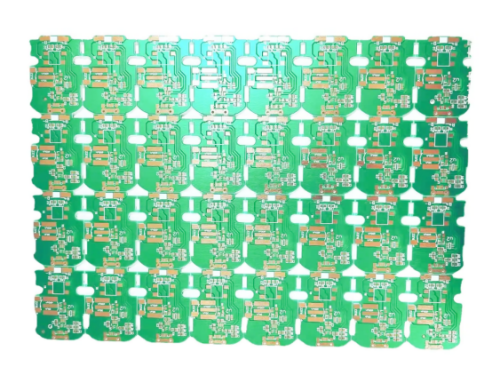
What Is RF PCB?
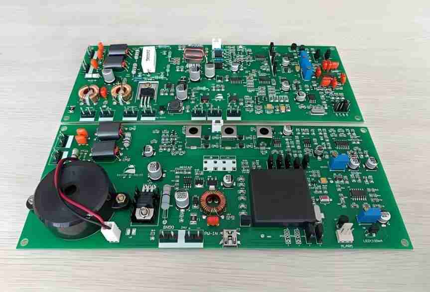
Table of Conent
Table of Conent
Are RF assemblies low-frequency or high-frequency? The operating frequency of RF components may range from very low frequencies up to extremely high frequencies. The RF range is 3kHz up to 300GHz. In practice however, the band from 3kHz up to 30MHz, for example, is low frequency, and is used for simple remote controls. The range between 30MHz-300GHz, is high-frequency.
What Is the Difference Between High and Low Frequency?
• Low-frequency circuits are used to process signals with lower frequencies. They typically range from tens of hertz to thousands. Common applications include audio circuits, etc.
• High-frequency circuits are used to process signals that have higher frequencies. These frequencies range from several kilohertz up to several hundred Megahertz. Satellites, radars and communications use high-frequency circuits.
Is the RF Assembly a High or Low Frequency?
High frequency is RF. This electromagnetic frequency can be transmitted into space. It ranges from 300kHz to 30GHz. Low-frequency currents are less than 1,000 variations a second. High-frequency currents can change 10,000 times per second. RF is included in high frequency currents.
RF PCB Basic Characteristics
• The range of RF frequencies is 300kHz to 30-GHz.The shorter the wavelength, the higher the frequency. The RF signal is higher in frequency and shorter in wavelength.
• The amplitude measures the change in oscillations of an electric field. The phase can be defined as a position at a single point in elongation.
• Modulation is required to modulate an RF signal. Data transmission also uses digital modulation. This technique, which utilizes frequency, phase and amplitude as well as frequency, phase and amplitude.
Definition of Frequency Range
• High-frequency signals are those that range between 3MHz to 300GHz. High-speed signals are PCB that have a frequency greater than 50MHz. Signals with edges less than 50ps high or low also fall into this category.
• Low-frequency signals are those between 100 Hz to 1000 kHz.
PCB Design Specific Applications
• The power supply in high-frequency designs is typically a layer which reduces noise, and minimizes loops. High frequency signals can cause interference. Noise is a factor that should be considered when designing.
• Low-frequency circuits do not require as much attention to noise or loops of signal, but they still need to be designed with electromagnetic compatibility and the integrity and strength of signals in mind.
What Is a PCB with High Frequency?
High-frequency printed circuit boards can operate between tens and hundreds of Megahertz. This PCB is perfect for efficient transmission. This PCB is ideal for efficient transmission. This PCB is made of special materials that ensure a low Dielectric Constant, which allows for high-speed communications. HF PCB is a flexible way to heat precision metals for processing. It can be used to heat components at various depths, depending on the application.
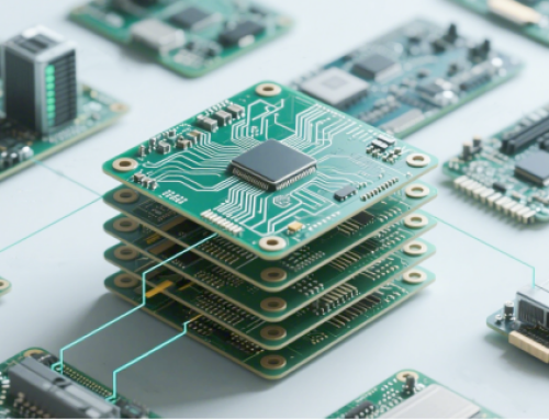
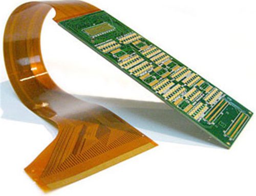
What Is RF PCB?
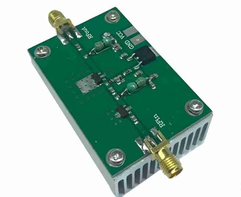
An RF PCB (Radio Frequency Printed circuit board) has to meet specific requirements in order to transmit high-frequency signals. This is important for shielding, minimizing interference, and isolating the circuit. The primary purpose of a RF PCB to reliably process high-frequency signal.
Considerations to Be Taken Into Account When Assembling RF PCB
1. RF PCB Assembly is a specialized field within the PCB industry. It requires a keen attention to detail and a thorough understanding of high-frequency signal.
2. The assembly of RF-PCB requires several considerations. Material selection, signal integrity and thermal management are among them. These factors are crucial to the overall performance of the RF System.
3. The selection of materials in RF PCB assembly is crucial.
4. The dielectric on the PCB can have a significant impact on signal transmission and loss characteristics. Dielectric loss can affect the integrity of high-frequency signals. Use materials with low dielectric constants. Most commonly used are ceramic-filled laminates and PTFE laminae. These materials provide good electrical performance across a range of frequencies. Copper foils for RF PCB should be smooth to reduce signal losses.
5. Signal integrity is another critical component of RF PCB assemblies that must be carefully managed. Reflections, electromagnetic interference (EMI) and crosstalk can affect high-frequency signals. This can negatively impact the performance of RF Circuits. These problems can be mitigated by using impedance control. Transmission lines must be precisely sized, positioned and maintained to ensure a constant impedance throughout the signal path. This is usually achieved by using microstrip and stripline technologies. Reduce EMI by using the right grounding and layering.
6. Both component placement and routing are important for RF PCB assembly. Plan the positioning of components to avoid distortion and signal loss. It is essential to place critical components such as antennas and connectors RF at the right places in order to optimize signal transmission. To minimize signal loss it is essential that high-frequency data be routed with minimal layer changes. Differential pair alignments and controlled impedance can be used to improve signal integrity.
RF PCB Assembly, as a result, is a demanding and complex process. This requires a lot of attention and knowledge about high-frequency signals. It is essential to consider key factors like material selection and thermal control when ensuring reliability and performance. The principles outlined here will enable manufacturers to create RF PCB which meet the high-frequency requirements of modern communication systems.
Common Challenges in RF PCB Design and Assembly
Designing and assembling RF PCB requires special knowledge.
1. When designing RF PCB, signal integrity is a key concern. Signal interference or loss of signals can affect performance. Designers must consider carefully the layout of the board, placement of components and routing traces to mitigate these issues.
2. To minimize signal attenuation, ensure that you use short and straight traces. To reduce electromagnetic interference, shielding and grounding layers can improve signal integrity.
3. Designers of RF PCB are also concerned about the challenge of matching impedance. Impedance mismatches can cause data errors and decrease the efficiency of an entire system. Designers must match transmission line impedances with connectors and components. Software or manufacturing processes can be used to achieve this.
4. Thermal management is a critical consideration when assembling RF PCB. Heat generated by high-frequency components can have a negative impact on the performance and reliability. To maintain optimal temperatures and dissipate the heat, heat management strategies such as heat vias or heat sinks are required. The life of a PCB can be reduced by improper heat management.
5. Materials are important in the design and assembly of RF PCB.The substrate material you choose can have a significant impact on PCB performance.Materials with low dielectric or angle of loss coefficients are ideal for high-frequency applications. These materials require expensive manufacturing equipment.
6. The complexity and miniaturization modern RF PCB makes assembly and design more challenging. The density of PCB will rise as devices get smaller and more integrated. Signal integrity will be more difficult to maintain and thermal issues will become more complex. To achieve high accuracy and reliability, advanced manufacturing techniques such as Microvia Surface Mount Technology (SMT), and other advanced technologies are required.
7. The RF PCB assembly includes testing and verification. PCB need to be able meet performance requirements under different conditions. This requires extensive testing including thermal tests and EMI tests as well as signal integrity tests. Testing will reveal problems that require design changes or modifications to assembly processes.
RF PCB assembly and design involves a complex interaction of factors, which must be managed carefully to achieve optimal performance. Each aspect of RFPCB construction and design is difficult, from signal integrity and impedance matching through to thermal management and materials selection. These challenges can be overcome by using advanced design techniques, precise production methods and thorough testing. High-quality RF PCB can be produced to meet modern application requirements.
Best Practices for RF PCB Component Placement
It is important to place components carefully in order to achieve the best performance and reliability when assembling RF PCB. Component placement is critical for RF circuits due to their complexity. Even minor errors in component placement can cause severe signal degradation and interference. It is essential to adhere to a few best practices during the design and assembly processes in order for you achieve optimal results.
1. You should first consider the integrity and safety of your signal path. The length of the path RF signals travel can affect their quality or cause interference. Designers can reduce signal attenuation by placing components close to one another. Maintaining a constant resistance along the path of the signal is essential. It is possible to achieve this by controlling the width, the space and the alignments of the board as well as the use of the right materials.
2. The management of electromagnetic interference is another critical element of RF PCB component design.EMI can seriously impact the performance of RF Circuits. Noise and distortion are the result. Place components in a way that minimizes the coupling between high- and low frequency signals. Shielding techniques are available to protect sensitive components against external interference.
3. Thermal management is a critical component of the assembly process for RF PCB. The heat generated by high frequency components can negatively impact their performance and life expectancy. Positioning components in a way that promotes heat dissipation is important. Heat sinks, vials or other cooling devices can be used. It is also important that components are spaced properly. This will reduce the chances of thermal coupling.
4. Consider the power integrity when RF PCB are being used.Power fluctuations can cause instability and noise.In order to maintain a constant supply of power, decoupling capacitances should be located as close as practicable to the power pins on active components. This will reduce noise and maintain voltage. Multiple grounding layers improve power distribution, reducing the risk of ground-loops.
5. Layout of passive components like resistors and capacitors also has a major impact on the performance of RF PCB. Place these components so that parasitic effects such as inductance or capacitance are reduced. These can change the behavior. Unwanted frequencies can be reduced by placing capacitors near the signal path. Inductors must be oriented in a way that minimizes mutual coupling.
6. It is essential to follow industry standards and guidelines when assembling RFPCB. IPC-2221 and IPC-2223 provide valuable insights into PCB design. They include the best practices in component placement and routing. These standards guarantee that a product will meet the performance and reliability requirements.
7. The placement of components in RF PCB assemblies is a critical and complex task that requires planning and attention. Designers who take into account factors like signal integrity, thermal control, and power integrity can optimize RF circuits. Adhering to industry guidelines and standards can improve the final product.These best practices can help you overcome challenges with RF PCB Assembly and improve performance.
8. Advanced Technologies for Signal Integrity & RF PCB. As devices become more complex, and operate at higher frequency, signal integrity becomes an increasingly important part of electronic design. To maintain RF signal fidelity and minimize interference, advanced techniques are required to ensure reliable performance.
9. Impedance plays a major role in the design of PCB used for RF.Signal reflections and data errors can be caused by impedance mismatches. Designers solve this problem by using controlled alignments. PCB traces need to be controlled precisely in terms of width and spacing if they are to maintain constant impedance values. This technique is particularly important for applications requiring high frequencies where even minor changes can have a major impact.
10. The correct grounding technique is another key technique. To minimize electromagnetic interference, a robust grounding layer must be used. Designers can make the ground plane continuous to improve signal integrity. The use of via splicing is also a way to improve grounding. Multiple vias are placed around the perimeter.
11. In RF PCB assembly, shielding is an important technique. Designers can protect components from electromagnetic fields by encapsulating shields. This will prevent the transmission of RF signals that could interfere with other components. This is especially important for densely packed PCB, where components are very close together and the chances of interference are higher. Shielding is only effective if it takes into account material and design factors.
12. Signal integrity is largely determined by the layout of the PCB. Avoid unnecessary loops or bends which can cause inductance. Signal quality can be affected. Designers simulate PCB designs to identify possible problems before manufacture. Designers can make early changes to the design.
13. It is important to select the right materials for RF PCB assembly. Dielectric properties are especially important for high frequency signals. Low dielectric coefficients and dielectric constants are the best materials. These properties reduce the signal attenuation. The most commonly used materials for RF PCB are PTFE (Teflon), ceramic-filled laminates and FR4 substrates. These materials have excellent electrical properties, but they can be difficult to work with.
14. To maintain the integrity of your signal, you must control and monitor the assembly process. It includes accurate placement of components, soldering and thorough inspections to detect any defects which could affect performance. To ensure high quality standards, advanced assembly techniques like Automated Optical Inspections (A.O.I.) or X.R. Inspections are employed.
Conclusion
In order to maintain signal integrity, RF PCB assembly requires impedance, shielding, optimizations, material choice and assembly techniques. With advancements in design techniques, designers can ensure that RF PCBs perform well in challenging applications. Careful layout and wiring are crucial to avoid signal integrity issues, especially when digital and RF signals interact.
Latest Blog

Contact Info
Phone: +86-755-82882936
Email: [email protected]
WhatsApp: +86-13570802455
Wechat: +86-13570802455
Address: 2nd floor,D Bldg.,Electric Link Technology Bldg.,Gongming,Guangming New Dist.,518106 Shenzhen, China