Multilayer PCB Basic Guide: Design to Production

Table of Conent
Table of Conent
In the realm of modern electronics, where miniaturization and high performance are paramount, the humble Printed Circuit Board (PCB) plays a foundational role. As devices become increasingly complex and compact, traditional single-layer and double-layer PCBs often fall short of meeting the demanding requirements. This is where the multilayer PCB steps in, offering a sophisticated solution for intricate electronic designs. A multilayer printed circuit board integrates multiple layers of conductive material, separated by insulating layers, to create a dense and highly functional electronic substrate. This basic guide will delve into the structure, benefits, design, fabrication, and applications of the essential multilayer PCB, providing a comprehensive understanding of multilayer circuit boards for both enthusiasts and professionals.
1. The Anatomy of a Multilayer Printed Circuit Board
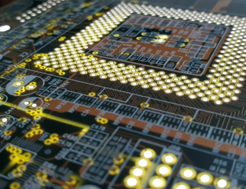
A multilayer PCB board is essentially a sandwich of alternating conductive and insulating layers. Unlike single or double-sided PCBs, which have conductive traces on one or both sides of a single substrate, multilayer boards incorporate three or more conductive layers within the board’s structure. The typical construction involves:
- Copper Layers:These are the conductive layers where traces , pads, and planes are formed. They are typically made from copper foil.
- Prepreg:A pre-impregnated material, usually fiberglass fabric impregnated with epoxy resin, which is partially cured. During the lamination process, heat and pressure cause the resin to flow and fully cure, bonding the layers together and forming the dielectric insulation between adjacent copper layers.
- Core:A fully cured laminate material, typically FR-4, with copper foil on both sides. Cores provide structural rigidity and are pre-bonded, unlike prepreg.
- Solder Mask:A protective layer applied to the outer surfaces of the PCB, usually green, which insulates the copper traces from environmental factors and prevents solder bridges during assembly.
- Silkscreen:A non-conductive ink layer used for printing component designators, logos, and other markings on the PCB surface.
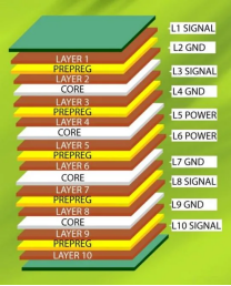
These layers are precisely stacked and bonded together under high temperature and pressure, creating a unified, robust structure. The arrangement of core and prepreg layers dictates the overall thickness and electrical properties of the multilayer board.
2. What are the Key Advantages of Multilayer Circuit Boards?
The adoption of multilayer PCBs stems from several compelling advantages that address the needs of modern electronics:
2.1 Space-Saving and Miniaturization
By routing traces on multiple internal layers, multilayer PCBs allow for significantly higher circuit density. This leads to smaller board sizes, which is crucial for compact electronic devices like smartphones, wearables, and medical implants. It’s a fundamental enabler of modern miniaturization trends.
2.2 Enhanced Performance and Speed
The ability to create dedicated ground and power planes within the internal layers provides excellent power distribution and reduces noise. Shorter signal paths possible with multilayer PCB design also lead to faster signal propagation, crucial for high-speed digital circuits and RF applications.
2.3 Improved EMI/EMC and Signal Integrity
Internal ground and power planes act as effective shields against electromagnetic interference (EMI), both emitting and absorbing. This improves electromagnetic compatibility (EMC) and helps maintain signal integrity, preventing cross-talk and ensuring cleaner signals, which is vital for sensitive circuits.
2.4 Better Impedance Control
The precise stacking of layers and controlled dielectric constants allow engineers to achieve accurate impedance control for high-frequency signals. This is critical for data transmission lines and RF components to prevent reflections and signal degradation.
2.5 Increased Durability
With multiple layers bonded together, multilayer circuit boards tend to be more robust and mechanically stable than their single or double-sided counterparts, offering greater resistance to environmental stress and physical impacts.
3. Challenges and Considerations for Multilayer PCB
While offering significant benefits, multilayer PCB manufacturing and use also present certain challenges:
- Increased Complexity and Cost:The intricate design and multilayer PCB production processes involve more steps and specialized equipment, leading to higher manufacturing costs and longer lead times.
- Design Intricacy:Designing multilayer boards requires sophisticated CAD tools and a deeper understanding of signal integrity, power integrity, and thermal management.
- Repair Difficulty:Due to the embedded layers, repairing internal traces or components on a multilayer PCB board can be extremely difficult or impossible once fabricated.
4. Multilayer PCB Design Principles
Effective multilayer PCB design is crucial for harnessing its full potential. Key considerations include:
1) Layer Stacking: The arrangement of signal, ground, and power layers significantly impacts performance. A common stack-up might involve outer signal layers, inner ground and power planes, and additional signal layers.
2) Via Types:
- ThroughHole Vias: Extend through all layers.
- Blind Vias:Connect an outer layer to an inner layer but do not go all the way through.
- Buried Vias:Connect two or more inner layers without reaching the outer layers.
3) Using blind and buried vias allows for even higher density routing by freeing up space on other layers.
4) Material Selection: The choice of core and prepreg materials (e.g., FR-4, high-Tg FR-4, low-loss materials) affects electrical performance, thermal properties, and cost.
5) Thermal Management: High-density designs can generate significant heat. Designing for effective heat dissipation, through thermal vias or dedicated planes, is essential.
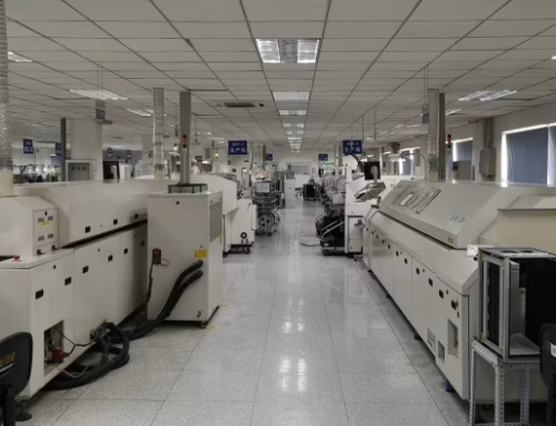
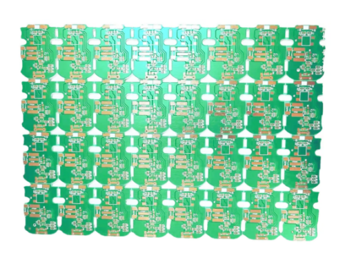
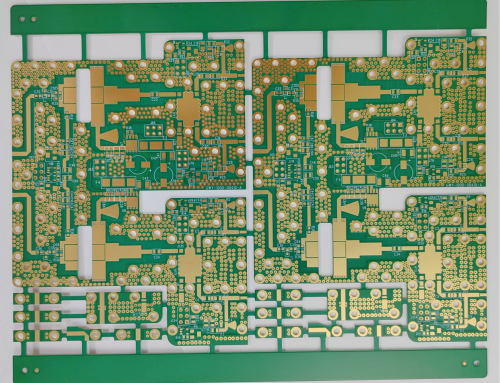
5. The Multilayer PCB Fabrication Process
Multilayer PCB fabrication is a complex, multi-stage process that requires precision and specialized equipment. Here’s a simplified overview:
1) Inner Layer Preparation: The inner copper layers are etched to create the desired circuit patterns. These patterns are then inspected.
2) Lamination: This is the core of multilayer PCB production. The treated inner layers are interleaved with prepreg and copper foils (for outer layers) and then subjected to high temperature and pressure in a laminating press. This process bonds all layers into a single, rigid structure.
3) Drilling: After lamination, holes (vias) are drilled through the board. These holes will later be plated to create electrical connections between layers.
4) Plating (Electroless & Electroplating): A thin layer of copper is deposited onto the hole walls (electroless plating), followed by thicker copper plating (electroplating) to ensure robust electrical connections.
5) Outer Layer Imaging and Etching: The outer copper layers are imaged and etched to form the external circuit patterns.
6) Solder Mask Application: A liquid or dry film solder mask is applied to the outer surfaces and cured to protect the copper traces.
7) Silkscreen Printing: Component designators and other markings are printed on the solder mask.
8) Surface Finish: A protective metallic coating (e.g., HASL, ENIG, OSP) is applied to exposed copper pads to ensure solderability and prevent oxidation.
9) Profiling and Testing: The board is routed or punched to its final shape. Electrical testing (e.g., flying probe, fixture test) is performed to check for opens and shorts.
Each step in multilayer PCB manufacturing is critical to the final quality and performance of the board.
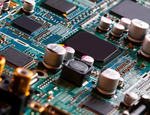
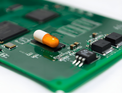
6. Applications of Multilayer PCBs
Multilayer printed circuit board technology is ubiquitous across a wide range of industries due to its ability to handle complex circuitry. Some common applications include:
- Consumer Electronics:Smartphones, tablets, smartwatches, digital cameras.
- Medical Devices:Pacemakers, diagnostic equipment, monitoring systems.
- Automotive:Engine control units (ECUs), infotainment systems, advanced driver-assistance systems (ADAS).
- Telecommunications:Routers, switches, base stations, servers.
- Aerospace and Defense:Avionics, radar systems, control systems .
- Industrial Control:Automation equipment, robotics, power supplies.
7. Choosing the Right Multilayer PCB Supplier
Selecting a reliable multilayer PCB supplier is paramount for successful project execution. Factors to consider include:
| Factor | Description | Benefit for You |
| Experience & Expertise | Years in business, specific experience with complex multilayer boards. | Reliable quality, fewer production issues. |
| Quality Certifications | ISO9001, IATF16949 (automotive), medical standards. | Adherence to high industry standards. |
| Manufacturing Capabilities | Number of layers supported, trace width/spacing, via types, material options. | Ability to meet your specific design requirements. |
| Lead Times | Typical turnaround for prototypes and production runs. | Timely project completion. |
| Cost-Effectiveness | Competitive pricing without compromising quality. | Optimized budget. |
| Customer Support | Responsiveness, technical assistance, DFM (Design for Manufacturability) guidance. | Smooth communication, help with design optimization. |
A good multilayer PCB supplier will not only provide competitive pricing but also offer technical support and ensure consistent quality, from prototyping to multilayer PCB production runs.
8. Multilayer PCB FAQs
Question1: What is the minimum number of layers for a PCB to be considered multilayer?
A PCB is generally considered a multilayer printed circuit board if it has three or more conductive layers, meaning at least two outer layers and one or more inner layers.
Question2: What are the most common materials used in multilayer PCB production?
The most common material is FR-4 (Flame Retardant type 4) for both core and prepreg due to its good balance of electrical, mechanical, and thermal properties. For high-frequency applications, specialized low-loss materials may be used.
Question3: Are multilayer boards always rigid?
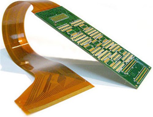
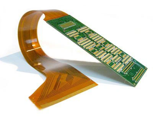
No, while rigid multilayer PCBs are most common, multilayer technology also extends to flexible PCBs and rigid-flex PCBs, combining the benefits of both rigid and flexible substrates.
Question4: How does a multilayer PCB help with electromagnetic interference (EMI)?
By incorporating dedicated ground and power planes, multilayer PCBs provide continuous, low-impedance paths for return currents and act as effective shields, absorbing and reflecting EMI, thereby significantly improving signal integrity and reducing noise.
Question5: What is the typical thickness of a multilayer PCB?
The thickness can vary widely based on the number of layers and material choices, ranging from very thin (e.g., 0.2mm for some flex-rigid boards) to several millimeters (e.g., 3.2mm or more for high-layer count boards). Common thicknesses include 1.6mm (0.062 inches) for standard boards.
9. Summary
The multilayer PCB is a cornerstone of modern electronic design, enabling the creation of compact, high-performance, and reliable devices. By stacking multiple layers of conductive and insulating materials, these boards overcome the limitations of simpler PCB types, offering superior signal integrity, power distribution, and EMI control. From intricate multilayer PCB design considerations like layer stacking and via selection to the precise steps of multilayer PCB fabrication, understanding this technology is essential for anyone involved in electronics manufacturing. The demand for these advanced boards continues to grow, making the selection of a capable multilayer PCB supplier and a thorough understanding of multilayer PCB production processes critical for success.
Key Takeaways
- Multilayer PCBs integrate three or more conductive layers for increased circuit density and functionality.
- They offer significant advantages in space-saving, performance, signal integrity, and EMI reduction.
- Multilayer PCB design requires careful consideration of layer stack-up, via types, and material selection.
- The multilayerPCB manufacturing process is complex, involving lamination, drilling, plating, and precise etching.
- Multilayer boardsare vital for a wide array of advanced electronics, from consumer gadgets to aerospace systems.
- Choosing an experienced and quality-focused multilayer PCB supplier is crucial for successful project outcomes.
Latest Blog

Contact Info
Phone: +86-755-82882936
Email: [email protected]
WhatsApp: +86-13570802455
Wechat: +86-13570802455
Address: 2nd floor,D Bldg.,Electric Link Technology Bldg.,Gongming,Guangming New Dist.,518106 Shenzhen, China