
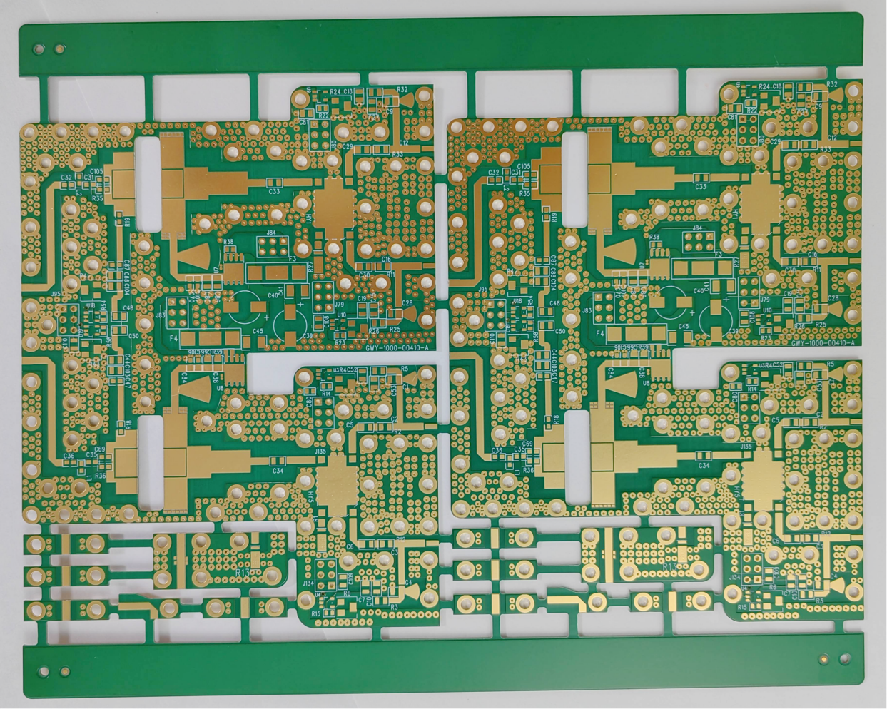

What is High Frequency PCB ?
High-frequency printed circuit boards (PCBs) play a crucial role in various advanced applications, especially in high-frequency PCB communication circuits, where signals operate at frequencies above 1 GHz. These PCBs have specific requirements and parameters that must be carefully considered during the design process to ensure optimal performance in communication systems.

Parameters To Consider For High-Frequency PCB Design:
Frequency Range: High-frequency PCBs typically operate above 1 GHz, with applications in radar systems, military equipment, aerospace, telecommunications, and high-speed digital systems.
Dielectric Constant (Dk): The dielectric constant of the PCB material affects the propagation speed of signals. Lower Dk values are preferred for high-frequency applications to minimize signal distortion and ensure accurate signal transmission.
Dissipation Factor (Df): Df represents the loss of signal energy as it travels through the PCB material. Lower Df values are desirable for high-frequency PCBs to reduce signal attenuation and maintain signal integrity.
Coefficient Of Thermal Expansion (CTE): CTE is crucial for high-frequency PCBs as it impacts the stability of the board’s dimensions under temperature variations. Low CTE materials help prevent issues like warping or delamination.
Signal Integrity: High-frequency PCB designs must minimize signal reflections, crosstalk, and electromagnetic interference (EMI) to preserve signal quality and reliability.
A High-Frequency PCB Requires the Use of Specialized Materials
Special materials are required to achieve the high frequency provided by this type of printed circuit board – any changes in the Er value of these materials can affect the impedance of the board. Many PCB designers turn to Rogers dielectric material for its lower dielectric loss, reduced signal loss, lower cost of circuit fabrication and better suitability for fast-turnaround prototyping applications.

RF PCB material, stackup and impedance decisions tied to the operating requirement
High-frequency PCB manufacturing controls the material system, copper geometry, reference planes, surface condition and fabrication tolerances that influence RF and microwave behavior. An RF PCB should be specified from the operating frequency, loss budget, impedance, power, thermal and environmental requirements rather than from a generic material brand alone. The laminate designation, dielectric data basis, copper profile, finished thickness, surface finish and controlled geometry all need to be part of the released package.
OrinewPCB reviews high-frequency PCB data before selecting a fabrication route and can coordinate the board with 100% new and original components, assembly and project-specific testing. This is valuable when RF connectors, controlled-impedance launches, shielding, grounding and component packages must match the bare-board construction and the final test boundary.
When should you choose High-Frequency PCB?
The correct route is the simplest construction that satisfies the released electrical, mechanical, thermal, compliance and assembly requirements. Use the comparison below to define why this board type is necessary before specifying details.
| Route | Use it when | Release decision |
|---|---|---|
| Conventional FR-4 route | Loss and dielectric variation remain acceptable for the actual channel | Validate with the real frequency, length and margin |
| Low-loss laminate | Insertion loss or phase stability requires controlled dielectric data | Specify material family, thickness and copper profile |
| Hybrid stackup | RF layers and conventional control layers need different materials | Define bonding, thermal expansion and stack symmetry |
| RF assembly program | Connector launch, shielding and component placement affect measured performance | Plan assembly, inspection and test fixtures with the PCB |
High-Frequency PCB design and DFM controls
The most useful DFM review checks the features that control fabrication and assembly risk, rather than comparing the design with a generic capability list.
Specify the electrical target
State impedance, tolerance, frequency range and the reference structure. A line width without its dielectric and plane context is incomplete.
Control the material identity
Use an exact material designation or an approved equivalence rule based on the required properties, not only the word Rogers or PTFE.
Review copper and finish effects
Copper profile, etch geometry and surface finish can influence conductor loss and launch consistency.
Protect the RF path during assembly
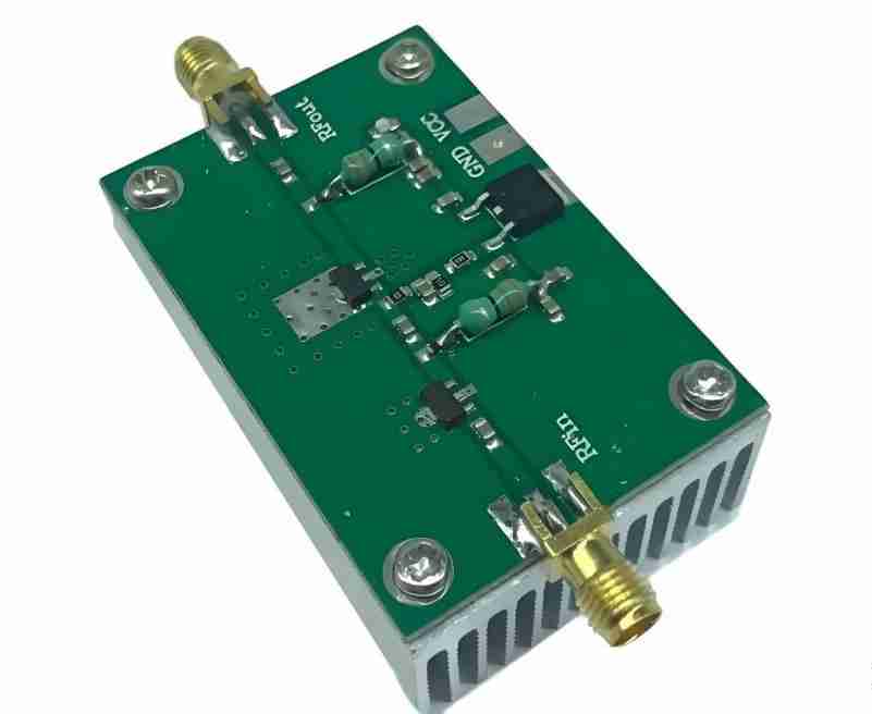
RF connectors, shields, grounding vias and sensitive networks need placement, soldering and cleaning requirements that match the design.
How the manufacturing route is reviewed
A reliable build keeps the requirement, material, fabrication data and acceptance evidence connected through the release process. The exact operations vary with construction, but the following gates should be explicit.
- Electrical requirement review: Translate frequency, loss and impedance requirements into a manufacturable stack.
- Material and stackup approval: Confirm laminate, bond material, copper and dielectric thickness.
- Impedance modeling: Review the controlled geometry and coupon or verification plan where required.
- Fabrication control: Manage patterning, lamination, drilling and finish for the released RF structure.
- Assembly interface review: Check launches, connector footprints, shielding and grounding features.
- Verification: Apply agreed board-level and functional RF evidence with a defined fixture and limits.
Files to send for an engineering review
Every file should identify the same board revision. A complete package shortens clarification time and makes price, material and delivery assumptions visible before production.
| Input | Required detail | Decision supported |
|---|---|---|
| Fabrication data | Gerber, ODB++ or IPC-2581 plus NC drill and board outline | Layer interpretation, holes, profile and DFM review |
| Stackup and materials | Layer order, finished thickness, copper, material and approved-equivalent rules | Construction and material proposal |
| Special requirements | Impedance, mechanical, compliance, finish, marking or documentation needs | Process selection and quotation scope |
| Assembly package | BOM, CPL, assembly drawing, variants and substitution rules when PCBA is required | Original-part sourcing and assembly planning |
| Test and delivery | Acceptance method, required evidence, quantity and target delivery | Inspection, test and schedule basis |
When the release package is ready, share the fabrication files and assembly inputs for a combined engineering review. OrinewPCB can then identify open DFM, material, sourcing and test questions before confirming the quotation scope.
High-Frequency PCB in one-stop PCB assembly
An RF PCB can pass bare-board electrical test and still miss system performance if connector launch, shielding, grounding or component installation is inconsistent. The one-stop PCB assembly scope can coordinate laminate, fabrication, original RF components, assembly controls and the customer-defined measurement plan.
Review Rogers PCB material planning and the site’s controlled-impedance capability guidance. The broader PCB manufacturing page explains the full fabrication-to-assembly path.
Quality, cost and lead-time factors
OrinewPCB uses a nine-step quality and test control framework that links release review, materials, fabrication, assembly and final verification. The actual inspection and test methods are selected for the board and customer-defined acceptance scope; not every board needs every method.
High-frequency PCB cost depends on laminate availability, hybrid construction, copper profile, controlled impedance, panel use, via structures, finish and the required verification. Material availability can control the schedule, so exact approved equivalents and required data should be resolved before release.
- Resolve missing or conflicting data before material is committed.
- Keep approved substitutions and evidence requirements in the released order.
- Confirm panel, tooling and assembly constraints together when PCBA is included.
- Plan delivery as early as practical after material, process and test inputs are reviewed.
High-Frequency PCB FAQ
What is a high-frequency PCB?
It is a printed circuit board whose material, geometry and fabrication controls are selected to meet defined RF or microwave performance requirements.
Is FR-4 suitable for every RF PCB?
No. FR-4 may be suitable when the actual loss, frequency, length and margin permit it. Higher-performance designs may require a controlled low-loss laminate.
What should an RF PCB quote package include?
Include the fabrication data, stackup, exact or approved material rule, impedance targets, copper and finish requirements, quantity and verification needs.
Can OrinewPCB assemble and test high-frequency boards?
Assembly and project-specific testing can be included when components, connectors, fixtures, methods and pass/fail limits are defined.
Plan the next build from one controlled data set
The board construction, component BOM, assembly revision and acceptance plan should describe the same product. This reduces supplier handoffs and makes engineering decisions easier to trace across prototypes, small-to-medium batches and high-mix production.
If the project is ready to move forward, provide the released PCB data, BOM, quantities and test requirements for the next-build review. The returned scope can address fabrication, 100% new and original component sourcing, assembly, testing and the earliest practical delivery plan together.