
Custom bare boards · fabrication review · one-stop PCBA
PCB Manufacturing and Fabrication Services
PCB manufacturing converts released design data into bare printed circuit boards through imaging, etching, lamination, drilling, plating, solder-mask, surface-finish, routing and inspection operations. A quote-ready project should define the board outline, copper layers, drill data, stackup or material requirements, copper weight, surface finish, impedance needs, quantity and acceptance expectations. OrinewPCB reviews these inputs before choosing a manufacturing route and confirming price or delivery.
For teams that also need components and assembly, the same project can continue as one-stop PCBA with 100% new and original component sourcing, SMT and through-hole assembly, and a nine-step quality and test control framework. This coordinated route is especially useful for small-to-medium batches and high-mix programs because it reduces supplier handoffs and keeps fabrication, BOM, assembly revision and test requirements aligned.
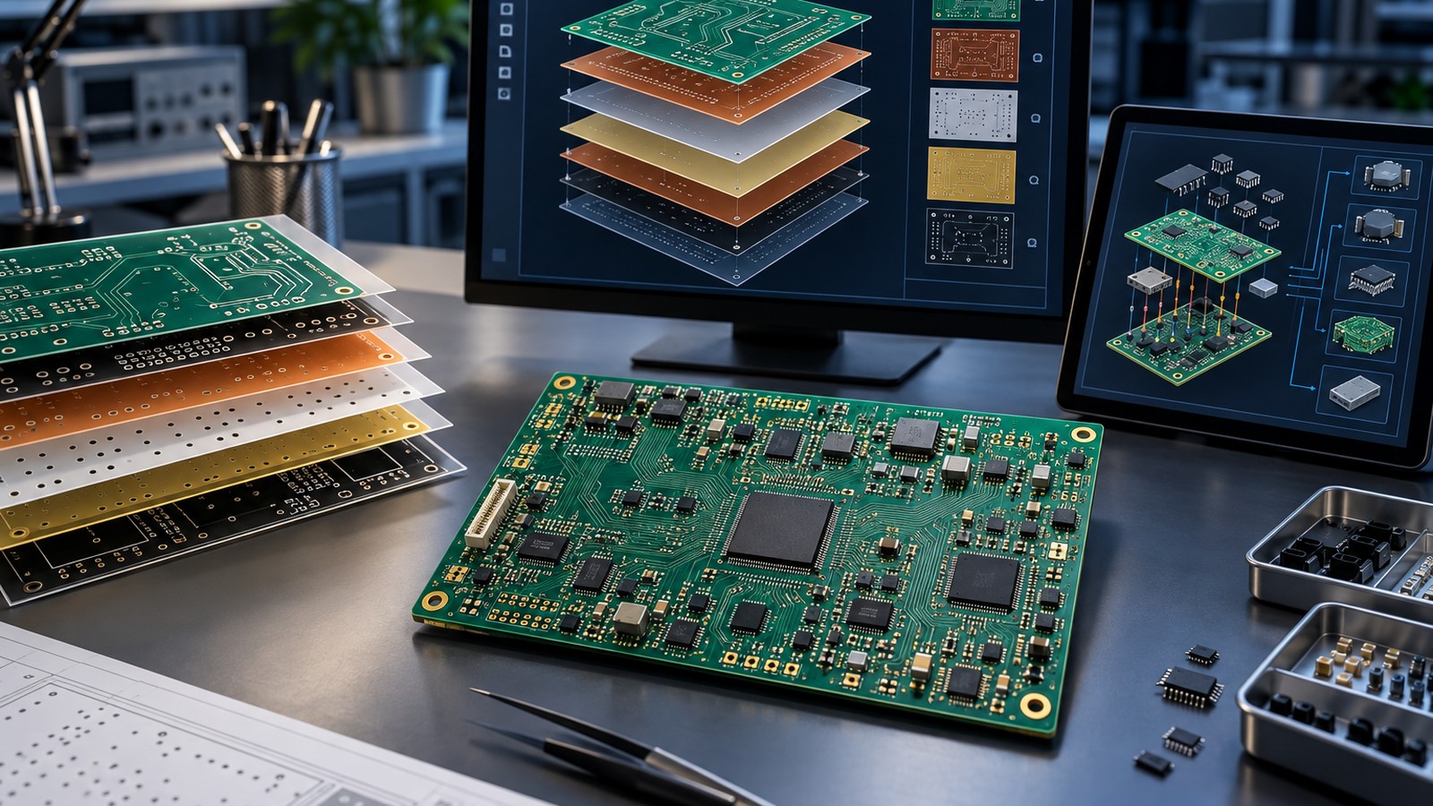
Fabrication data first
Construction, material, finish and special-process choices are reviewed against the released files before production.
Built for product variety
Prototype, small-to-medium batch and high-mix programs can be planned without assuming one construction fits every board.
One-stop path available
Bare-board fabrication can continue into original-part sourcing, assembly and project-specific test under one coordinated scope.
Choose the right scope
PCB fabrication, assembly and one-stop PCBA are different deliverables
A PCB manufacturer produces the unpopulated board. PCB assembly adds sourced or consigned components. One-stop PCBA coordinates the board, BOM, component supply, assembly, inspection and agreed testing so the interfaces are managed together.
| Scope | What is delivered | What you provide | Best fit |
|---|---|---|---|
| Bare PCB manufacturing | Fabricated, finished and inspected unpopulated boards | Gerber or ODB++, drill, stackup notes, quantity and board acceptance requirements | Teams with their own component sourcing and assembly capability |
| PCB assembly | Components placed and soldered on customer-supplied or separately sourced boards | BOM, CPL, assembly drawing, boards, components and test instructions as applicable | Programs with a controlled material kit and known assembly route |
| One-stop PCB assembly | PCB fabrication, original component sourcing, assembly, inspection and agreed testing | One aligned fabrication, BOM, placement, drawing, quantity and acceptance package | Small-to-medium batches, many variants and teams seeking fewer supplier handoffs |
A one-stop order does not remove engineering decisions. It gives one team responsibility for identifying mismatches early—for example, a footprint that does not match the selected component, a surface finish that does not suit the assembly plan, or test coverage that requires additional access.
Quote-ready manufacturing package
Send the files that control the board, not only a PCB screenshot
Complete fabrication data reduces assumptions in price, construction and schedule. Export all layers from the same released revision and include a readme for requirements that are not unambiguous in the data.
| Input | Minimum useful content | Decision supported |
|---|---|---|
| Gerber, ODB++ or IPC-2581 | All copper, solder-mask, silkscreen, paste and mechanical layers from one revision | Image generation, layer interpretation and DFM review |
| NC drill and route data | Plated and non-plated holes, slots, cutouts and finished board profile | Drilling, plating, routing and dimensional review |
| Stackup and material notes | Layer order, target thickness, copper weight, material class and controlled dielectric needs | Construction proposal and material selection |
| Impedance requirements | Target impedance, tolerance, reference layer and relevant trace geometry | Stackup and coupon planning where required |
| Finish and marking | Surface finish, mask and legend colors, date or lot marking, and special notes | Finish route and final appearance |
| Quantity and panel needs | Boards per revision, array preference, rails, breakaway method and assembly constraints | Panel utilization, tooling and production planning |
| Acceptance requirements | Applicable workmanship class, inspection records and any customer-defined limits | Inspection plan and quotation scope |
Useful first review
Send the fabrication files, quantity and target delivery for a PCB manufacturing review. If assembly is also required, attach the BOM, pick-and-place data, assembly drawing and test requirements so the quotation can cover the full project rather than only the bare board.
Manufacturing flow
How released PCB data becomes a finished bare board
The exact route varies by layer count and construction. The sequence below shows the major control points without implying that every board uses the same materials or special processes.
-
Engineering review
Check file completeness, outline, drill data, annular features, spacing, stackup notes and special requirements.
-
Inner-layer imaging
Transfer the released copper pattern to prepared laminate, develop it and etch away unwanted copper.
-
Layup and lamination
Align inner layers with prepreg and copper, then laminate the stack under a controlled cycle.
-
Drilling and plating
Create holes and slots, prepare hole walls and plate the conductive path required by the construction.
-
Outer-layer patterning
Image, plate and etch the external copper features before mask application.
-
Mask, legend and finish
Apply solder mask, legend and the selected surface finish according to released notes.
-
Profile and separation
Route or score the board or production panel while maintaining the approved outline and array rules.
-
Electrical and visual checks
Use the agreed bare-board electrical test and visual or dimensional checks appropriate to the order.
-
Final verification
Confirm identification, quantity, required records and packaging before the lot is released.
Construction route
Select PCB technology from the product need—not from a capability list
Layer count alone does not define manufacturability. Electrical performance, current, bend behavior, heat flow, component pitch, thickness and assembly method all affect the practical construction.
| Technology route | Use it when | Key review inputs |
|---|---|---|
| Four-layer PCB | Power and ground planes, routing density or EMC control exceed a simple two-layer layout | Stack order, finished thickness, copper distribution and via strategy |
| HDI PCB | Fine-pitch devices, routing escape or size constraints justify microvias and sequential structures | Microvia structure, capture pads, build-up sequence and reliability evidence |
| Heavy copper PCB | Higher current or heat-spreading needs justify increased copper weight | Finished copper, spacing, etch compensation, thermal relief and assembly compatibility |
| High-frequency PCB | Insertion loss, dielectric stability or RF behavior drives the material and geometry | Material designation, dielectric data, impedance, copper profile and finish |
| Rigid-flex PCB | Rigid component areas and flexible interconnects must form one controlled circuit | Flex stack, bend region, stiffener, coverlay, transition and assembly handling |
| Flexible or metal-core PCB | Bending, packaging or heat-transfer requirements call for a nonstandard rigid-board route | Material system, mechanical boundary, insulation or thermal assumptions and end-use constraints |
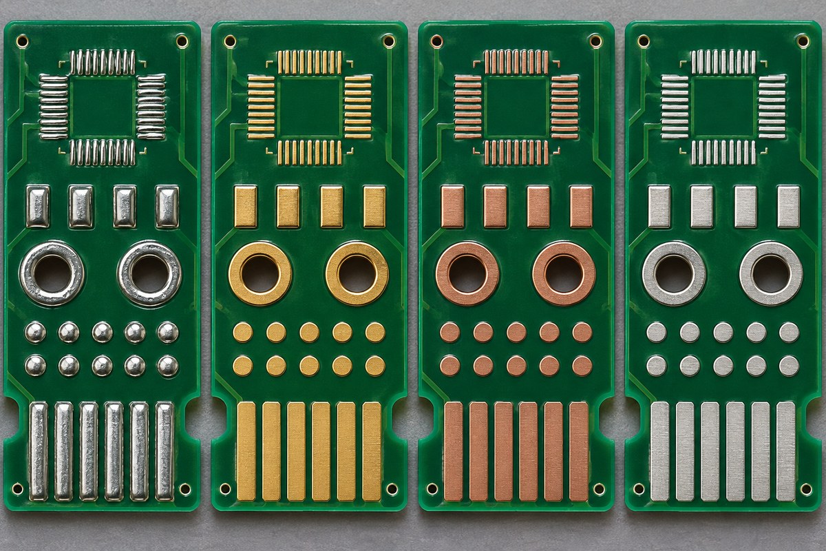
Finish, material and stackup are connected decisions
ENIG, HASL, OSP and immersion finishes do not provide the same flatness, storage behavior or contact characteristics. Likewise, specifying only “FR-4” may not be enough when thickness, thermal behavior, loss, flame performance or controlled dielectric data matter.
State the functional requirement and allow the manufacturing review to identify any missing parameter. This produces a more useful answer than copying a generic capability table into the drawing.
Quality controls
A nine-step quality and test framework connects design release to shipment
OrinewPCB uses a nine-step quality and test control framework. The specific inspection, measurement and test methods depend on the construction and the customer-approved scope; no single checklist can prove every board characteristic.
-
Release alignment
Verify that fabrication files, drawings, notes, revision and quantity agree.
-
DFM review
Check geometry, hole structures, edge features, copper balance and missing requirements.
-
Material review
Confirm the proposed laminate, copper, finish and documented substitutions against the order.
-
Inner-layer control
Inspect the patterned inner layers before they are enclosed by lamination.
-
Lamination and drill control
Monitor the construction route and verify critical registration or drilling conditions.
-
Plating and outer-layer checks
Review the conductive build and visible pattern features at the applicable stages.
-
Mask, legend and finish review
Check coverage, registration, marking and the selected final finish.
-
Electrical and dimensional verification
Apply the agreed bare-board test and relevant outline, hole or feature checks.
-
Final release
Confirm workmanship, identity, quantity, required records and protective packaging.
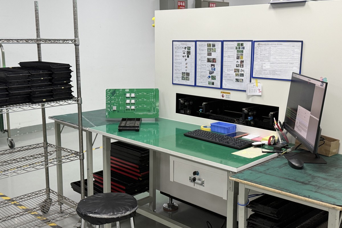
Quality needs a measurable acceptance statement
Useful requirements identify the characteristic, limit and evidence. Examples include a target impedance and tolerance, a finished board dimension, an electrical test requirement, a specified marking, or an agreed inspection record.
Terms such as “high quality” or “100% tested” are incomplete unless the test boundary is defined. The quotation should state what is included and which customer inputs remain open.
From bare board to assembled product
One-stop PCB assembly reduces handoffs for small-to-medium, high-mix programs
The greatest coordination benefit comes after fabrication: the approved board revision, component BOM, placement data, assembly drawing and test plan stay under one project control.
100% new and original components
OrinewPCB’s sourcing policy is to use new and original parts. Manufacturer and established distributor relationships support availability review, competitive material pricing and lead-time visibility. Any proposed alternate still requires controlled approval.
High-mix release control
Different revisions, population variants and quantities need explicit identifiers. One-stop management helps prevent a fabrication revision, BOM option or assembly program from being applied to the wrong lot.
Assembly and test planning
SMT, through-hole, manual operations, AOI, X-ray, electrical and functional checks are selected according to package mix, access, risk and the accepted test definition.
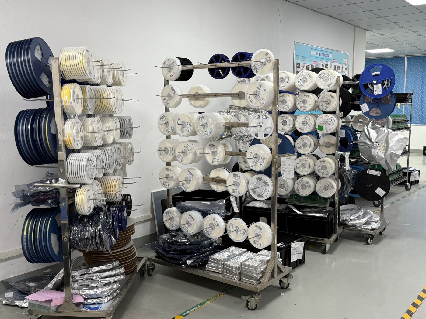
Do not let component availability become a late-stage surprise
A complete BOM should name the manufacturer, exact manufacturer part number, package, quantity per board and substitution rule. Ambiguous descriptions can create cost, schedule and fit risks even when the PCB itself is manufacturable.
For a combined board, sourcing and assembly scope, review the turnkey PCB assembly service. It explains how fabrication, component purchasing, assembly and testing can be coordinated under one order.
Price and delivery basis
What changes PCB manufacturing cost and lead time?
Price and delivery are outputs of the released construction, not universal promises. The earliest practical schedule can be confirmed after file review, material availability and production requirements are understood.
- Layer count, board size and panel utilization
- Material system, finished thickness and copper weight
- Hole count, aspect ratio and special via structures
- Trace/space, annular geometry and impedance control
- Surface finish, mask, legend and edge requirements
- Quantity, test scope, records and packaging
How to improve quote accuracy
- Remove obsolete notes and duplicate file revisions.
- State target values and tolerances, not only preferred process names.
- Separate required characteristics from optional preferences.
- Provide prototype and expected repeat quantities.
- Identify the target assembly route and panel constraints.
Fast is useful only when the release is buildable
OrinewPCB plans delivery as early as practical, but incomplete files, material substitutions, engineering questions or revision changes can move the schedule. Resolving them before release protects both speed and quality.
Common questions
PCB manufacturing FAQ
What is the difference between PCB manufacturing and PCB assembly?
PCB manufacturing produces the bare circuit board. PCB assembly mounts and solders components onto that board. One-stop PCBA coordinates both stages plus component sourcing and the agreed inspection or test scope.
Which files are needed for a PCB fabrication quote?
Provide Gerber, ODB++ or IPC-2581 data, NC drill files, board outline, layer or stackup notes, material and finish requirements, quantity, and any impedance or acceptance requirements. All files should carry the same revision.
Can OrinewPCB manufacture prototypes and small batches?
Prototype and small-to-medium quantities can be reviewed. Practical routing depends on the board construction, material, panel use, engineering setup and any special test or record needs.
Can you also source components and assemble the boards?
Yes. A one-stop scope can include PCB fabrication, 100% new and original component sourcing, SMT and through-hole assembly, inspection and project-specific testing.
How is surface finish selected?
The choice depends on pad flatness, storage, soldering, contact use, wire bonding if applicable, cost and other project requirements. State the functional need so the finish can be reviewed with the assembly plan.
How quickly can PCBs be delivered?
Delivery depends on construction, material availability, quantity, special processes, inspection and open engineering questions. OrinewPCB confirms the earliest practical schedule after reviewing the released package.
Start with one controlled revision
Request a PCB manufacturing or one-stop PCBA review
Tell OrinewPCB whether the project stops at bare boards or continues through component sourcing, assembly and test. A complete release package lets the team separate confirmed scope from open questions and respond with a more reliable price and delivery basis.
- Gerber/ODB++/IPC-2581
- NC drill and board outline
- Stackup, material and finish
- Quantity by revision
- BOM with exact MPNs
- Pick-and-place and drawing
- Test and acceptance criteria
- Target delivery and packaging
What happens next?
- File and revision alignment is checked.
- PCB construction and DFM questions are identified.
- If assembly is included, BOM availability and approved sourcing rules are reviewed.
- Inspection and test assumptions are clarified.
- The quotation states included scope, open items and schedule basis.
No matching PCB manufacturing video was found on the official @OrinewPCB YouTube channel during this update, so no unrelated video was embedded.