

What is HDI PCB?
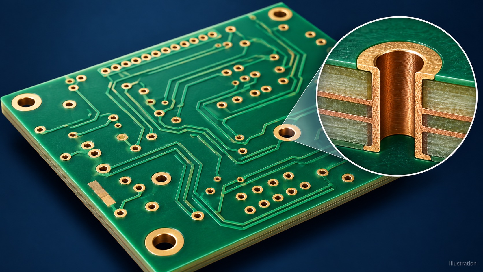
HDI stands for High Density Interconnector. A circuit board which has a higher wiring density per unit area as opposed to conventional board is called as HDI PCB. HDI PCBs have finer spaces and lines, minor vias and capture pads and higher connection pad density. It is helpful in enhancing electrical performance and reduction in weight and size of the equipment. HDI PCB is the better option for high-layer count and costly laminated boards.
The emergence of HDI technology has propelled the development of the PCB industry by enabling the integration of denser components like BGAs and QFPs.

High-density interconnect structures for constrained routing and package escape
HDI PCB manufacturing uses fine features, microvias and controlled build-up structures to increase routing density compared with a conventional through-hole multilayer board. A high-density interconnect PCB is justified when component pitch, breakout, board area or interconnection performance requires it; HDI should not be selected only because it sounds more advanced. The stackup, microvia type, sequential lamination plan, capture pads, dielectric materials and reliability expectations must be reviewed together.
OrinewPCB reviews HDI fabrication data before the build and can continue the project into one-stop PCB assembly. For small-to-medium batches and high-mix products, keeping the HDI stack, exact component packages, assembly drawing and test plan under one revision reduces the risk that a package escape or via-in-pad decision is separated from the assembly process it must support.
When should you choose HDI PCB?
The correct route is the simplest construction that satisfies the released electrical, mechanical, thermal, compliance and assembly requirements. Use the comparison below to define why this board type is necessary before specifying details.
| Route | Use it when | Release decision |
|---|---|---|
| Conventional multilayer | Through vias can complete routing without unacceptable board area or stubs | Use the simpler stack when it meets density and performance needs |
| 1+N+1 HDI | One build-up layer on each side resolves fine-pitch escape | Define laser vias, capture pads, dielectric and via fill |
| Multi-step HDI | Several build-up layers or stacked structures are required | Sequential lamination, registration and reliability evidence become critical |
| Rigid-flex or advanced package route | Mechanical folding or package architecture changes the interconnect system | Review the complete mechanical and assembly boundary |
HDI PCB design and DFM controls
The most useful DFM review checks the features that control fabrication and assembly risk, rather than comparing the design with a generic capability list.
Use an explicit microvia structure
State whether vias are staggered, stacked, filled or placed in pads. Do not leave the fabricator to infer the build from Gerber alone.
Balance routing density and reliability
Adding build-up layers can solve escape routing but also increases process steps, cost and the need for validated reliability assumptions.
Coordinate via-in-pad with assembly
Filled and capped pads affect planarity, paste printing and hidden-joint inspection for fine-pitch BGAs.
Control stackup and impedance together
Fine features, dielectric thickness and reference planes influence both manufacturability and electrical performance.
How the manufacturing route is reviewed
A reliable build keeps the requirement, material, fabrication data and acceptance evidence connected through the release process. The exact operations vary with construction, but the following gates should be explicit.
- Package and escape review: Confirm which devices and routing channels require HDI.
- Stackup definition: Release the build-up sequence, materials, copper and impedance requirements.
- Core fabrication: Pattern the core layers that form the central multilayer structure.
- Laser drilling and via formation: Create and plate the specified microvia structures for each build-up cycle.
- Sequential lamination: Add the released dielectric and copper layers in the approved sequence.
- Final inspection and test: Apply agreed electrical, dimensional and microsection evidence where required.
Files to send for an engineering review
Every file should identify the same board revision. A complete package shortens clarification time and makes price, material and delivery assumptions visible before production.
| Input | Required detail | Decision supported |
|---|---|---|
| Fabrication data | Gerber, ODB++ or IPC-2581 plus NC drill and board outline | Layer interpretation, holes, profile and DFM review |
| Stackup and materials | Layer order, finished thickness, copper, material and approved-equivalent rules | Construction and material proposal |
| Special requirements | Impedance, mechanical, compliance, finish, marking or documentation needs | Process selection and quotation scope |
| Assembly package | BOM, CPL, assembly drawing, variants and substitution rules when PCBA is required | Original-part sourcing and assembly planning |
| Test and delivery | Acceptance method, required evidence, quantity and target delivery | Inspection, test and schedule basis |
When the release package is ready, share the fabrication files and assembly inputs for a combined engineering review. OrinewPCB can then identify open DFM, material, sourcing and test questions before confirming the quotation scope.
HDI PCB in one-stop PCB assembly
HDI boards are often paired with fine-pitch packages, so board fabrication cannot be isolated from assembly access, paste design and inspection coverage. The turnkey PCB assembly route lets the HDI construction, 100% new and original component sourcing, placement data and test expectations be reviewed as one release.
Compare the HDI route with a conventional four-layer PCB stackup and review rigid-flex PCB manufacturing when the density problem is also mechanical. The parent PCB manufacturing service explains the wider fabrication scope.
Quality, cost and lead-time factors
OrinewPCB uses a nine-step quality and test control framework that links release review, materials, fabrication, assembly and final verification. The actual inspection and test methods are selected for the board and customer-defined acceptance scope; not every board needs every method.
HDI cost and lead time rise with sequential lamination count, microvia complexity, via filling, fine geometry, material selection, panel utilization and the required evidence. Reducing the number of build-up cycles can have more impact than small changes to board outline.
- Resolve missing or conflicting data before material is committed.
- Keep approved substitutions and evidence requirements in the released order.
- Confirm panel, tooling and assembly constraints together when PCBA is included.
- Plan delivery as early as practical after material, process and test inputs are reviewed.
HDI PCB FAQ
What is an HDI PCB?
An HDI PCB is a high-density interconnect board that uses fine features and microvia-based build-up structures to increase routing density.
When should I use HDI instead of a conventional multilayer PCB?
Use HDI when package escape, board size, routing density or electrical constraints cannot be met efficiently with through vias and a conventional stack.
What files are needed for HDI PCB manufacturing?
Provide the complete fabrication data, explicit stackup, microvia structure, materials, copper, impedance requirements and any required inspection evidence.
Can HDI boards be assembled as a turnkey project?
Yes. The board, original components, fine-pitch assembly, inspection and agreed test scope can be coordinated under one controlled project.
Plan the next build from one controlled data set
The board construction, component BOM, assembly revision and acceptance plan should describe the same product. This reduces supplier handoffs and makes engineering decisions easier to trace across prototypes, small-to-medium batches and high-mix production.
If the project is ready to move forward, provide the released PCB data, BOM, quantities and test requirements for the next-build review. The returned scope can address fabrication, 100% new and original component sourcing, assembly, testing and the earliest practical delivery plan together.