
OrinewPCB · Built around your product requirements
Custom PCB Assembly Services
Custom PCB assembly matches PCB fabrication, components, assembly and testing to your released design. OrinewPCB provides one-stop PCBA with 100% new original components, especially for high-mix, low- and medium-volume orders.
Send the BOM, board files, assembly requirements and quantity for each model. We review feasibility, material cost, quality requirements and your target date together before confirming the quotation and delivery plan.
- Prototype to repeat production
- 100% new original parts
- Nine-step quality workflow
One team for the whole build
Coordinate bare boards, component supply, SMT/THT assembly and agreed testing through one project team.
Original parts, competitive sourcing
Deep cooperation with manufacturers and distributors supports genuine materials, favorable BOM pricing and availability.
Quality and delivery together
Our nine-step quality workflow and your acceptance requirements inform the production and shipment plan.
Tailored PCB solutions
What can be customized in your PCB assembly project?
Customization starts with the electrical, mechanical and operating requirements of your product. PCB materials and construction, component population, assembly methods and verification should be reviewed together.
Material selection
Specify the laminate, copper weight, thermal requirements and any special material constraints. FR-4 is commonly used for rigid boards; polyimide constructions can be used for flexible designs. Material choice must fit the stack-up and intended environment.
Layer configuration and stack-up
Single-sided, double-sided and multilayer constructions have different routing, power and fabrication implications. Provide the required stack-up, finished thickness and any impedance targets for review.
Soldermask and silkscreen
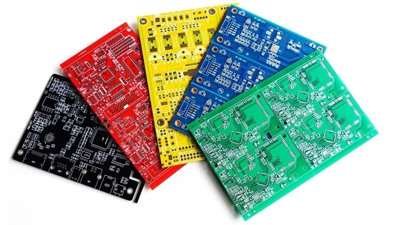
Define mask color, surface finish, component markings, polarity and revision identification. Clear assembly markings support inspection and service; visual choices must remain compatible with manufacturing requirements.
Component population and assembly
Define one- or two-sided SMT, through-hole parts, mixed assembly, DNP positions and mechanical requirements. The appropriate soldering and handling sequence depends on the complete board.
Use the PCB manufacturing capability overview for fabrication planning. For package and process detail, review the SMT assembly and through-hole assembly requirements alongside your BOM.
High mix · Small and medium batches
Keep every model, BOM and revision clearly defined
A multi-variant order needs a controlled configuration for each model, even when most components are shared. Identify differences before sourcing or setup so the right parts, firmware and tests are applied to each build.
| Project input | What to define | Why it matters |
|---|---|---|
| Model and quantity | Unique model name, revision and order quantity for each variant. | Separates material allocation, setup and delivery requirements. |
| Shared and changed components | Matching reference designators, exact part numbers and a clear variant BOM or difference list. | Prevents assuming that similar boards have identical component populations. |
| DNP and substitutions | Do-not-populate positions, approved alternatives and approval rules. | Keeps sourcing changes consistent with the intended configuration. |
| Programming and acceptance | Firmware revision, programming instructions and pass/fail limits by model. | Prevents a correctly assembled board from receiving the wrong firmware or test. |
| Mechanical requirements | Connector orientation, mounting details, enclosure constraints and special assembly notes. | Checks that the finished assembly fits the actual product. |
For connected and IoT devices, identify module variants, power configurations, firmware versions and the interfaces required for testing. For prototype-to-production changes, release the new files and identify what changed. A previous successful build does not automatically validate a different component, footprint or test requirement.
Engineering reference
PCBA specifications to confirm for your design
The specification references below support initial engineering discussions. Confirm the actual board, package combination, tolerances and applicable production conditions with the project team before finalizing your order.
| Item | Reference specification | Project-specific confirmation |
|---|---|---|
| Assembly configuration | Single- or double-sided SMT; through-hole and mixed assembly. | Review component mix, board-side access and soldering sequence. |
| PCB dimensions | 50 × 50 mm to 610 × 508 mm. | Confirm finished-board versus panel dimensions, handling and tooling requirements. |
| PCB thickness | 0.5–4.5 mm. | Confirm construction, material, handling and the proposed assembly route. |
| BGA diameter / spacing | 0.2 mm / 0.35 mm. | Supply the package drawing and land pattern; confirm how these dimensions apply to the actual device. |
| QFP width / spacing | 0.15 mm / 0.25 mm. | Confirm lead geometry and the meaning of width and spacing from the supplier drawing. |
| Placement accuracy reference | < ±30 μm under the listed conditions of 3σ and Cpk ≥ 1. | Equipment-related reference; not a finished-product tolerance or a guarantee for every package. |
| Placement-rate reference | 600,000 chips/hour. | Confirm the equipment scope of this throughput reference. Setup, board mix and tests determine actual order output. |
| Quality-system reference | ISO 9001:2015. | Request the current certificate and applicable scope if required for supplier qualification. |
| Delivery | Confirmed after file, material and test review. | Provide your target date. Delivery is quoted for the complete project rather than a universal fixed number of days. |
If your board is outside a listed reference, send the requirements for review. A package’s pitch, lead dimensions and solder-ball diameter are different measurements; do not substitute one for another when checking feasibility.
100% new original components
Build the quality plan around the product’s requirements
OrinewPCB emphasizes quality through original component sourcing and a nine-step inspection and testing workflow. The applicable methods, acceptance criteria and records are agreed for the actual assembly.
Authentic components and sourcing value
Our manufacturer and distributor relationships support original electronic components, competitive material cost and practical supply schedules. Provide approved manufacturer part numbers and substitution rules.
Revision and process control
Use consistent fabrication files, BOMs, placement data and drawings. Highlight critical parts, thermal restrictions, special handling and any differences between models. Projects with programmed placement and inspection should also define the automated PCB assembly route for each model.
Acceptance defined before production
Specify functions, electrical checks, programming, fixtures and reporting needs. Medical, automotive, aerospace or other regulated applications require their applicable quality and documentation requirements to be reviewed explicitly.
| Verification area | Methods or requirements to discuss | Scope to confirm |
|---|---|---|
| Assembly condition | Visual inspection, AOI and selected hidden-joint inspection where applicable. | Accessible features, package types, acceptance criteria and reinspection. |
| Electrical assembly checks | Flying-probe or fixture-based electrical testing, as appropriate. | Test access, electrical coverage, programs and pass/fail limits. |
| Product operation | Programming and functional testing under defined conditions. | Firmware, input/output interfaces, loads, fixtures and expected behavior. |
| PCB fabrication properties | Impedance testing, hole-resistance measurements or microsection analysis where specified. | The fabrication characteristic being checked, sampling and required records. |
| Special material or reliability evaluation | Solderability or thermal-shock requirements where applicable. | Purpose, sample plan, conditions, acceptance limits and whether testing is destructive. |
These are different verification purposes, not a claim that every board receives every method. Fabrication tests and reliability evaluations do not replace functional testing of the completed product.
From requirements to shipment
A coordinated custom PCBA build process
A successful custom build needs a clear scope and approved files before production. The same review should cover board fabrication, components, assembly, quality and the required delivery date.
-
Review the design and requirements
Check the released files, quantities, mechanical needs and acceptance scope. Resolve unclear dimensions, material notes, package information and variant differences.
-
Confirm components and the quotation
Review original-part availability, approved alternatives, fabrication requirements, assembly work and test preparation. Confirm the complete quoted scope and practical schedule.
-
Prepare and assemble
Use the agreed fabrication data, BOM, placement information and work instructions. Define the appropriate SMT, through-hole and additional assembly operations.
-
Inspect, program and test
Carry out the agreed checks and programming. Investigate discrepancies, control rework and complete the applicable reinspection or retest.
-
Accept and arrange delivery
Confirm quantity by model, required records, packing and shipment. Retain clear revision identifiers for any repeat order or subsequent engineering change.
Cost and material availability
Control engineering changes and repeat orders
For every change, identify the affected revision, BOM references, placement data, firmware and test limits. Agree the approval point before procurement or assembly, and confirm how existing inventory, fixtures and work in progress will be handled. Keep the released configuration distinct from a proposed alternative.
What determines the custom assembly price?
Compare the total project cost using the same released BOM, board requirements, quantities and test scope. A price based only on board area misses most assembly and procurement differences.
- PCB materials, stack-up, dimensions and fabrication requirements.
- Original component pricing, availability and approved alternatives.
- Component population, package mix, sides and special operations.
- Setup effort spread across quantities and product variants.
- Programming, fixtures, testing and documentation.
Our sourcing relationships help support favorable material pricing and lead times. Any proposed substitution should be reviewed for the product before it is used to change the quotation.
A practical delivery plan
How can the project move sooner?
Complete files and early material decisions reduce avoidable delays. We work toward the earliest practical delivery date while preserving the agreed quality scope.
- Release matching files and identify unfinished information.
- List the quantity and revision for each model.
- Flag long-lead parts and approve alternatives explicitly.
- Provide firmware, test procedures and the required delivery date.
Our quick-turn review checks the complete fabrication, material and assembly requirements before a schedule is confirmed.
Start a custom one-stop assembly inquiry
Ask for non-recurring engineering (NRE), stencil, programming and fixture costs to be identified separately from recurring build costs. Confirm reuse and any changes needed for a repeat order. For sourcing choices, see turnkey PCB assembly; for multiple models in small batches, see low-volume, high-mix PCB assembly.
Send the build package for one model or several variants
Provide the available files and identify any missing information. OrinewPCB will review fabrication, original components, assembly feasibility, inspection and testing, cost and delivery as one project.
- PCB files: Gerbers, drill files, stack-up, material and fabrication notes.
- BOM: manufacturer part numbers, references, quantities, DNP positions and approved alternatives.
- Assembly package: placement/CPL data, drawings, polarity, mechanical requirements and variant differences.
- Order and acceptance: quantity and revision by model, firmware, test requirements, records and target date.
Custom PCB assembly FAQ
Questions before a custom build
What materials are used in custom printed circuit boards?
A PCB combines conductive copper, a dielectric substrate or laminate, soldermask and identifying markings. FR-4 is commonly used for rigid construction, while flexible boards may use polyimide. Copper weight, material grade and layer construction must match the application; they do not alone determine product power consumption.
Can you handle small orders with several different board models?
Yes. High-mix, low- and medium-volume one-stop PCBA is a core focus. Provide the quantity, revision and component differences for each model so materials, setup and testing can be reviewed correctly.
Can soldermask color and silkscreen be customized?
Specify your preferred color and marking requirements in the fabrication package. Confirm availability and any process constraints, and keep polarity, reference designators and revision markings readable.
Can you review a replacement board when the original files are missing?
Share the available board information, photographs, drawings, known components and test requirements. Any reverse-engineering or file-reconstruction scope needs separate feasibility review; a board image alone is not a complete manufacturing package.
Do the reference package dimensions guarantee my design can be assembled?
No. Feasibility depends on the actual package drawing, land pattern, board construction, process access and acceptance criteria. Send the specific device and layout information for review.
How is a repeat order or design change handled?
Identify the approved revision and provide an explicit change list. Confirm BOM substitutions, DNP positions, firmware and test changes rather than assuming the previous build instructions remain valid.
Related assembly services