
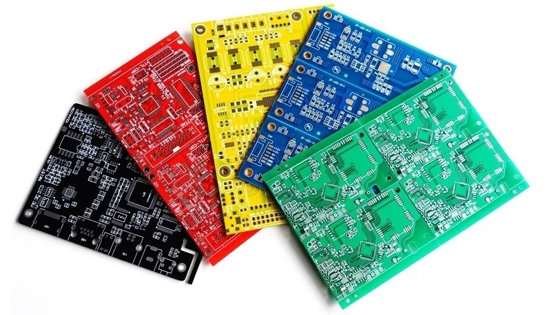
Ceramic PCB: material and manufacturing decisions
A ceramic PCB uses a ceramic substrate, such as alumina or aluminum nitride, with a compatible conductor or metallization system. It is a different construction from an aluminum-base insulated metal substrate. Material grade, metallization route, thickness, mounting and assembly method determine whether it suits the application. A ceramic material name alone does not establish finished-board thermal resistance, reliability or the manufacturer’s process capability.
Specify the construction before comparing suppliers
Compare alumina and aluminum nitride PCB options using the exact supplier grade and product architecture. Thermal conductivity, expansion behavior, mechanical strength and cost must be considered alongside the conductor system and attachment method. DBC, AMB and thick-film routes are different manufacturing approaches, not interchangeable labels for every ceramic PCB. Confirm the proposed process before artwork release. Ceramic handling also needs attention to brittle fracture, edge damage, mounting stress and solder-joint strain.
| Design route | Decision | What to confirm |
|---|---|---|
| Alumina substrate | A ceramic route with a defined grade and cost target | Confirm purity, thickness, metallization and mounting |
| Aluminum nitride substrate | Thermal requirements justify reviewing an AlN option | Use supplier-specific material data and process availability |
| Conductor / metallization | Electrical and attachment requirements define the route | Confirm the proposed process rather than assuming DBC or AMB |
| Power module assembly | Die attach, soldering and housing stress interact | Release attachment, test and mechanical requirements together |
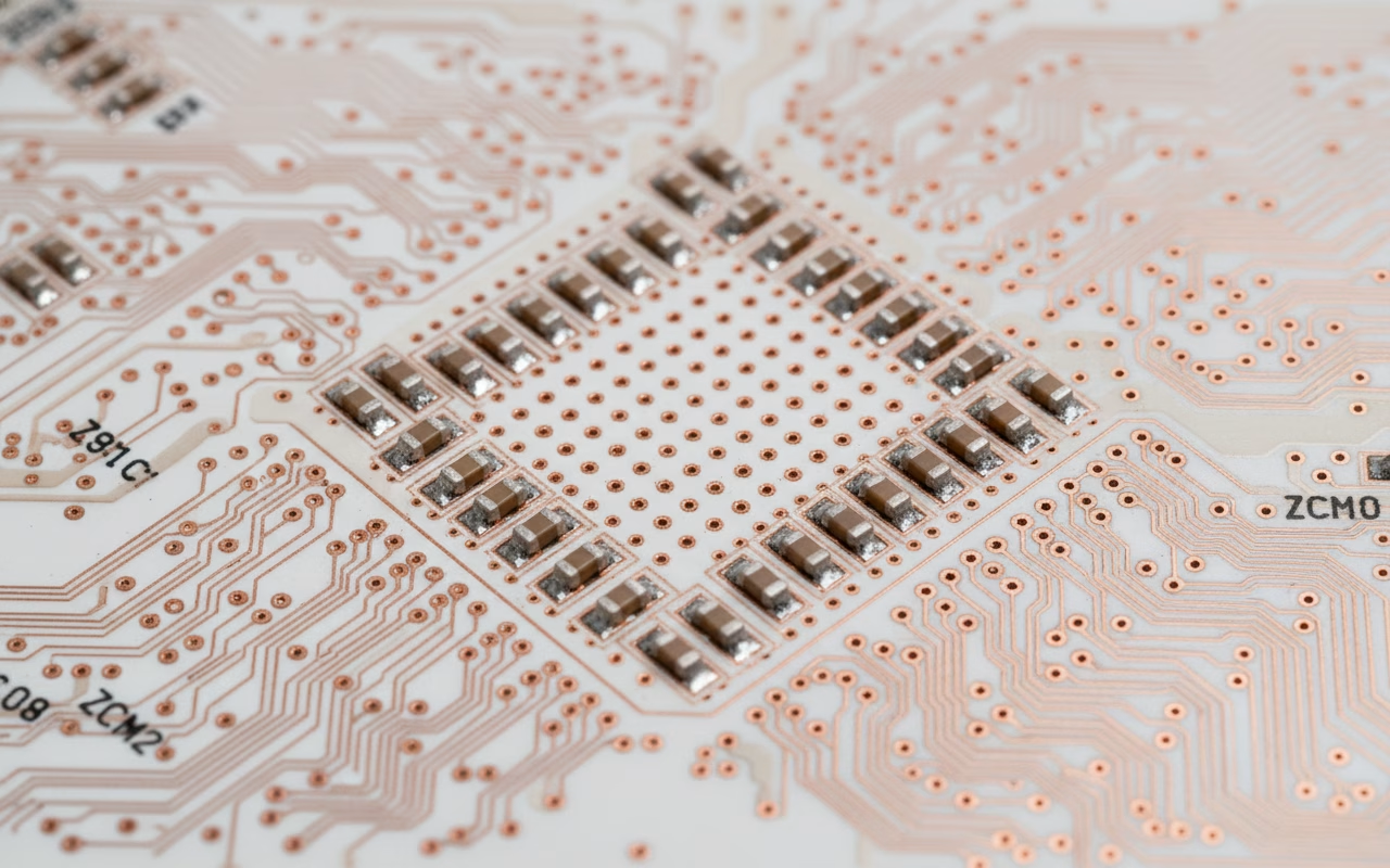
Compare related routes when the design needs a different balance of electrical, thermal and mechanical performance: metal core PCB alternatives; aluminum-base board planning; heavy copper power-board construction. Material selection should close against an approved drawing, not a generic capability list.
For a construction assessment, share the stackup, fabrication data and application constraints with quantities and the target date. The review can identify open material, geometry and manufacturing questions before a combined quotation is prepared.
Ceramic PCB assembly and original component sourcing
Ceramic PCB assembly should be reviewed before the substrate construction is committed. Component attachment, pad finish, soldering or other joining methods, fixture support and the housing interface can all affect the finished assembly. Define the electrical, programming and functional checks separately from any environmental qualification. A ceramic PCB manufacturer needs more than an outline and material name: conductor data, metallization, mechanical tolerances and acceptance evidence must describe the same deliverable.
OrinewPCB focuses on one-stop PCB assembly, particularly small-to-medium batches and high-mix builds. The turnkey PCB assembly workflow connects board fabrication, 100% new and original component sourcing, assembly and the agreed tests. Manufacturer and distributor relationships support BOM pricing and material planning; exact availability, approved alternates and delivery dates are confirmed for each released revision.
Quality evidence and the nine-step workflow
OrinewPCB uses a nine-step quality and test workflow. The project plan must specify the actual inspections, electrical tests, programming and functional checks that apply to the build. Do not treat a generic test count as evidence that every possible test is performed on every product. Record the acceptance criteria, inspection coverage, required documentation and any agreed sampling plan before production begins.
Keep PCB, BOM, placement and assembly drawing revisions consistent. Record approved substitutions against exact manufacturer part numbers, and separate customer-supplied parts from sourced parts. High-mix programs need clear variant quantities, do-not-populate positions and firmware versions so similar boards do not enter the wrong assembly or test route.
Cost, delivery and the complete build package
Material availability, board size, panel utilization, copper, holes, surface finish, assembly tooling and test preparation all contribute to cost and lead time. The earliest practical delivery depends on resolving these inputs together. A bare-board price cannot represent a finished PCBA price unless components, assembly and testing are explicitly included.
For an assembled-board assessment, supply Gerber or ODB++ data, the fabrication drawing, BOM with manufacturer part numbers, pick-and-place data, assembly drawings, quantities, variant details and the required test limits. Identify the intended environment and any special evidence requirements. This allows purchasing and engineering decisions to be reviewed before materials are committed.
A ceramic PCB manufacturer should confirm the exact substrate and metallization route. Supplier references such as CoorsTek alumina materials and CeramTec aluminum nitride substrates help distinguish material families; they are not evidence that every grade or process is available for a specific order.
Ceramic PCB purchasing question
Is ceramic PCB thermal expansion always high?
No. Expansion depends on the ceramic grade and surrounding materials. Review expansion mismatch across the substrate, conductor, component attachment and housing rather than relying on a generic high or low claim.
The right construction is the one that meets the released electrical, thermal, mechanical and acceptance requirements. When the project is ready to proceed, provide the coordinated fabrication and assembly files so OrinewPCB can review the complete PCBA scope and material schedule together.