
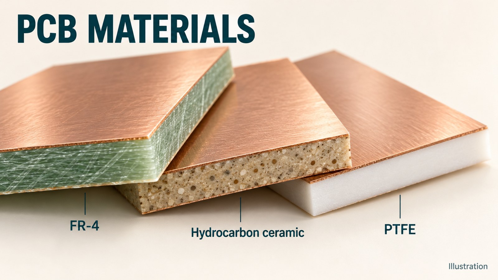

What is Halogen free PCB?
Halogen free PCB is a printed circuit board non-contain any halogen elements, During PCB manufacturing, the concerned halogen elements like Chlorine and Bromine do have some benefits however these do not outweigh their negative impact that can be caused in our day to day life.
What is a Halogen?
Halogens are a class of reactive elements in group 17 on the periodic table.
These elements exhibit high reactivity and are commonly used in many chemical compounds across industries.
Halogen-Free Materials
• Halogen-Free Laminate
In halogen-free PCB, laminate is used for the substrate. Usually, it is halogen-free FR4, where FR stands for flame retardant material. Below are the alternatives for both flame retardant and resin.
Flame Retardants:
Several brominated compounds are used in traditional PCBs, such as PBB, PBDE, TBBPA, and HBCD. In halogen-free printed circuit boards, these compounds are replaced by the following halogen-free flame retardant additives.
• Aluminum (aluminum hydroxide, aluminum diethyl phosphinate)
• Phosphorus (phosphorus-based FR4 materials, phosphorus-based flame retardants)
• Magnesium hydroxide
• Ceramics
• Melamine derivatives
Epoxy Resin:
FR4 halogen-free laminates use epoxy resin. It is typically a thermosetting polymer that provides mechanical stability and insulation. Traditionally, this resin contains halogens. In halogen-free boards, the resins used are usually the following:
• Benzoxazine resin
• Bismaleimide triazine
• trifunctional epoxy resin
• Bisphenol Epoxy Vinyl Ester
• Cyanate
• Polyimide
• Halogen-Free Flux
Halogenated solder paste or flux is used to assemble circuit boards. This solder paste contains a bromine activator and helps remove oxidation during the soldering process while also providing sanding properties. In the halogen-free solder, flux has been replaced by safer options.

Material compliance defined by the released laminate and declaration scope
Halogen-free PCB manufacturing uses laminate and related material systems that meet the project’s specified halogen limits and declaration requirements. “Halogen-free” should not be treated as a color, a general environmental claim or a substitute for an exact material specification. The customer must define the applicable requirement, evidence and scope—bare laminate, finished PCB, assembled board or finished product—because those boundaries do not automatically mean the same thing.
OrinewPCB reviews the released PCB material requirement and can coordinate the bare board with 100% new and original components, assembly and project-specific testing. For a one-stop PCBA, compliance evidence must cover the agreed project boundary and remain linked to the actual material and component revisions used in the build.
When should you choose Halogen-Free PCB?
The correct route is the simplest construction that satisfies the released electrical, mechanical, thermal, compliance and assembly requirements. Use the comparison below to define why this board type is necessary before specifying details.
| Route | Use it when | Release decision |
|---|---|---|
| Conventional laminate | No halogen restriction applies to the released product | Specify normal electrical, thermal and reliability requirements |
| Halogen-free PCB material | A customer, market or product requirement defines halogen limits | Name the standard or declaration basis and required evidence |
| Halogen-free assembled board | The requirement extends beyond laminate to solder mask, components or process materials | Define the PCBA boundary and supplier declarations |
| Finished-product compliance | The final device carries the obligation | Coordinate enclosure, cables, labels and other non-PCB materials separately |
Halogen-Free PCB design and DFM controls
The most useful DFM review checks the features that control fabrication and assembly risk, rather than comparing the design with a generic capability list.
Define the compliance boundary
State whether the requirement applies to laminate, finished board, assembled PCBA or the complete product.
Approve the exact material
Use a released laminate designation and evidence package. Do not accept an undocumented swap because both materials are described as halogen-free.
Review thermal processing
Material selection must still support lamination and assembly thermal cycles for the actual stack and component mix.
Keep declarations linked to the lot
Supplier documentation is useful only when it identifies the applicable material, revision and scope.
How the manufacturing route is reviewed
A reliable build keeps the requirement, material, fabrication data and acceptance evidence connected through the release process. The exact operations vary with construction, but the following gates should be explicit.
- Requirement review: Identify the applicable limit, product boundary and required declaration.
- Material proposal: Select a laminate and supporting materials that match electrical, thermal and compliance needs.
- Document approval: Confirm acceptable evidence before fabrication release.
- Board fabrication: Build the approved stack without undocumented material substitution.
- Assembly boundary review: Extend sourcing controls when the PCBA must meet the same requirement.
- Final record check: Release the agreed material and lot evidence with the order.
Files to send for an engineering review
Every file should identify the same board revision. A complete package shortens clarification time and makes price, material and delivery assumptions visible before production.
| Input | Required detail | Decision supported |
|---|---|---|
| Fabrication data | Gerber, ODB++ or IPC-2581 plus NC drill and board outline | Layer interpretation, holes, profile and DFM review |
| Stackup and materials | Layer order, finished thickness, copper, material and approved-equivalent rules | Construction and material proposal |
| Special requirements | Impedance, mechanical, compliance, finish, marking or documentation needs | Process selection and quotation scope |
| Assembly package | BOM, CPL, assembly drawing, variants and substitution rules when PCBA is required | Original-part sourcing and assembly planning |
| Test and delivery | Acceptance method, required evidence, quantity and target delivery | Inspection, test and schedule basis |
When the release package is ready, share the fabrication files and assembly inputs for a combined engineering review. OrinewPCB can then identify open DFM, material, sourcing and test questions before confirming the quotation scope.
Halogen-Free PCB in one-stop PCB assembly
A halogen-free bare board does not automatically make every component, cable, connector or process material in the assembled product halogen-free. When the obligation extends to PCBA, the BOM and approved sources must carry the same boundary. The turnkey PCB assembly workflow can connect material evidence, original component sourcing and build records under one controlled order.
Compare the material decision with FR-4 PCB selection and high-Tg PCB planning. The PCB manufacturing service explains how the material requirement fits the full build.
Quality, cost and lead-time factors
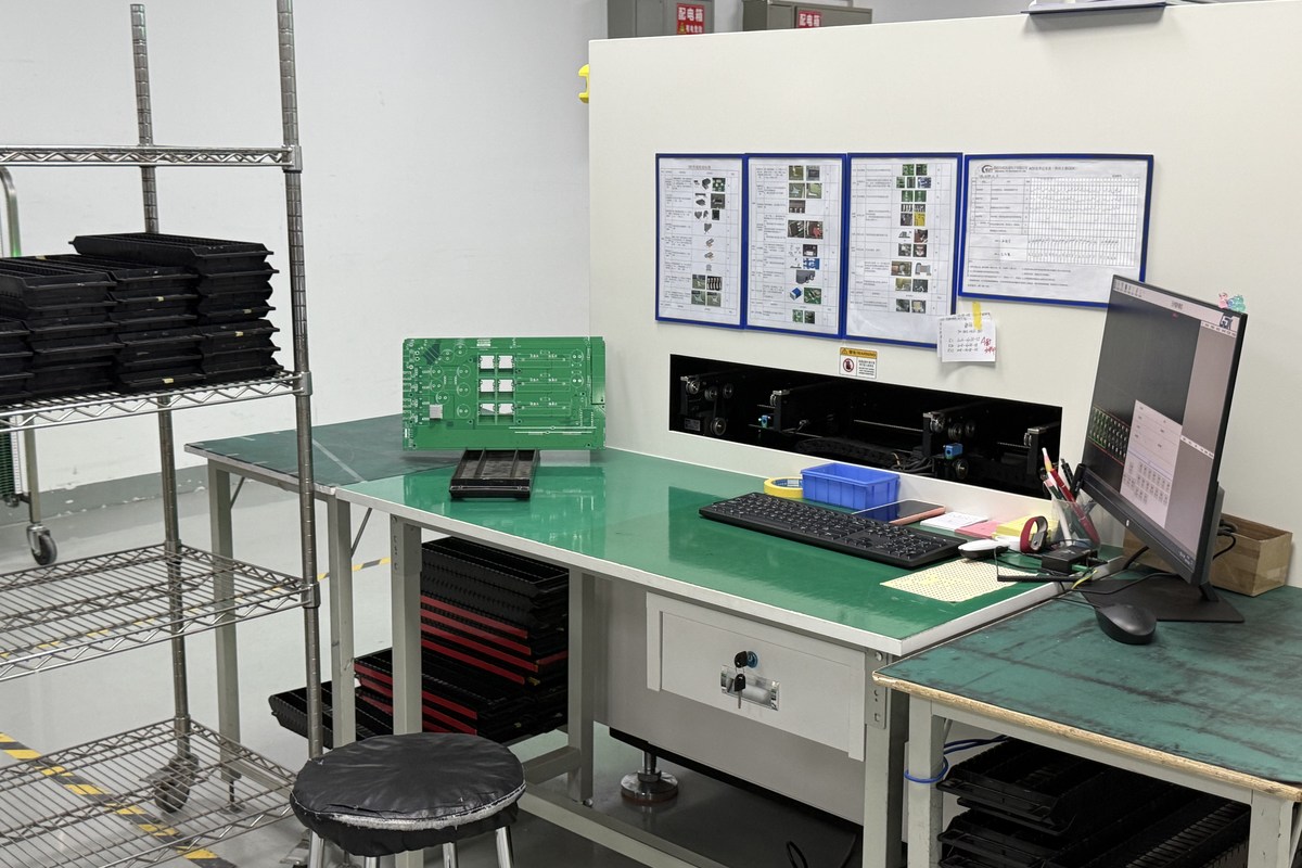
OrinewPCB uses a nine-step quality and test control framework that links release review, materials, fabrication, assembly and final verification. The actual inspection and test methods are selected for the board and customer-defined acceptance scope; not every board needs every method.
Cost and lead time depend on approved laminate availability, stackup, copper, finish, documentation and whether the requirement extends into assembly. Defining acceptable equivalents and evidence before release avoids late material changes that can disrupt both fabrication and sourcing.
- Resolve missing or conflicting data before material is committed.
- Keep approved substitutions and evidence requirements in the released order.
- Confirm panel, tooling and assembly constraints together when PCBA is included.
- Plan delivery as early as practical after material, process and test inputs are reviewed.
Halogen-Free PCB FAQ
What is a halogen-free PCB?
It is a PCB built with materials that meet a specified halogen requirement within a defined scope. The applicable limit and evidence should be stated in the order.
Does a halogen-free PCB make the whole product halogen-free?
No. Components, cables, connectors, process materials and the enclosure may have separate compliance requirements.
What evidence should be requested?
Request the material identification and declarations or test evidence required by the applicable customer or product specification.
Can halogen-free boards be assembled as a turnkey project?
Yes, when the BOM, approved sources, assembly materials and documentation boundary are defined before purchasing and production.
Plan the next build from one controlled data set
The board construction, component BOM, assembly revision and acceptance plan should describe the same product. This reduces supplier handoffs and makes engineering decisions easier to trace across prototypes, small-to-medium batches and high-mix production.
If the project is ready to move forward, provide the released PCB data, BOM, quantities and test requirements for the next-build review. The returned scope can address fabrication, 100% new and original component sourcing, assembly, testing and the earliest practical delivery plan together.