
Heavy-current PCB planning · DFM before release
Heavy Copper PCB Manufacturing
A heavy copper PCB—also called a thick copper PCB—uses increased copper thickness on selected or all conductive layers to create a larger conductor cross-section and improve heat spreading. It is commonly evaluated for power conversion, motor control, power distribution and other high-current circuits. Copper weight alone does not determine safe current or temperature: trace width, layer position, ambient conditions, allowed temperature rise, stackup and cooling path all matter.
OrinewPCB reviews the released fabrication data, finished copper requirement for each layer, geometry, materials, drill and plating notes, surface finish and acceptance criteria before confirming manufacturability, price or schedule. If assembly is included, the thermal mass and soldering route are reviewed with the BOM and component limits.
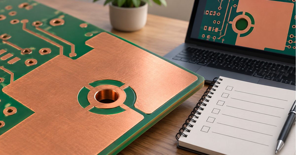
Specify finished copper by layer
State the required finished value and tolerance instead of writing only “heavy copper.”
Size conductors for the real thermal case
Current, temperature rise, copper geometry, layer position and cooling must be evaluated together.
Plan fabrication and assembly together
Etching, resin fill, drilling, solder mask and soldering behavior can all change with copper mass.
Definition and selection
What “heavy copper” should mean in your fabrication package
Commercial definitions vary. A practical design conversation often starts around 3 oz/ft² (approximately 105 µm), but a purchase specification should never depend on that informal cutoff. Record the finished copper target for every conductive layer and separate conductor copper requirements from plated-hole requirements.
Use it for a defined electrical or thermal need
Choose thicker copper when conductor cross-section, voltage drop, localized heat spreading or robust power interconnection requires it. Avoid adding copper weight as a substitute for current and thermal analysis.
Keep fine signal routing separate where practical
Thicker copper is harder to etch into fine features. A mixed stackup may keep selected power layers heavy while allowing signal layers to use geometry appropriate to their function, subject to stackup and fabrication review.
Define acceptance, not just construction
Identify the applicable drawing notes, finished copper requirement, electrical test, dimensional controls and any microsection or coupon evidence needed for the order.
| Nominal copper weight | Approximate thickness | How to use the value |
|---|---|---|
| 1 oz/ft² | 35 µm (0.035 mm) | Common reference point; not normally described as heavy copper. |
| 2 oz/ft² | 70 µm (0.070 mm) | Heavier than standard constructions, but terminology varies by supplier. |
| 3 oz/ft² | 105 µm (0.105 mm) | A frequently used starting point for “heavy” or “thick” copper discussions. |
| 4 oz/ft² | 140 µm (0.140 mm) | Expect wider manufacturable spacing than on thinner copper layers. |
| 6 oz/ft² | 210 µm (0.210 mm) | Requires early confirmation of etch geometry, resin fill, drilling and stackup. |
| 10 oz/ft² | 350 µm (0.350 mm) | Design reference only; availability and combinations must be confirmed for the actual construction. |
Conversions are nominal planning values. Starting foil, plating and finished copper are not interchangeable terms. Put the required finished value and tolerance on the fabrication drawing.
Engineering inputs
Release the electrical, thermal and fabrication requirements together
The right copper weight depends on what the board must do and how it will be cooled. Before layout release, capture the operating current, duty cycle, ambient range, allowed temperature rise, conductor geometry and any enclosure or heat-sink interfaces.
| Input | Decision it supports | What to document |
|---|---|---|
| Current and duty cycle | Conductor cross-section and expected loss | Continuous, peak and transient current; duration; repetition and simultaneous loads. |
| Temperature limits | Allowable conductor heating | Ambient range, maximum board or conductor temperature and allowed temperature rise. |
| Layer position | Heat transfer and current-capacity assumptions | External or internal layer, adjacent planes, dielectric thickness and copper balance. |
| Electrical spacing | Insulation and manufacturing clearance | Working voltage, transient conditions, pollution or coating assumptions and applicable safety rules. |
| Thermal path | Heat spreading and removal | Copper area, thermal vias, component pad, chassis or heat-sink interface, airflow and enclosure conditions. |
| Drill and plating | Connection between copper layers | Finished hole sizes, via strategy, annular rings, hole-wall requirements and press-fit needs if any. |
| Assembly scope | Soldering and inspection route | BOM, thermal-sensitive components, pad geometry, solder process, test access and acceptance criteria. |
Use IPC-2152 as a design reference—not a substitute for validation
IPC-2152 addresses current-carrying capacity in printed board design. Its methods still need the real board geometry and thermal environment. Prototype measurement or simulation may be appropriate when the allowed temperature rise or current margin is critical.
For the broader board build, review the released stackup with our PCB manufacturing service before locking fine features or unusual layer combinations.
Design for manufacturability
The main heavy copper PCB DFM risks appear at the interfaces
Thick copper changes more than trace resistance. It affects etching, clearances, lamination topography, resin fill, drilling, plating, solder mask and the thermal behavior seen later in assembly.
| DFM area | Why it changes with thick copper | Recommended release action |
|---|---|---|
| Trace and spacing | More copper must be removed during etching, increasing the importance of etch compensation and conductor profile. | Confirm minimum width and spacing for each finished copper thickness before routing is frozen. |
| Pad and annular ring | Clearance and registration margins can be consumed by thicker copper geometry. | Review pad sizes, antipads, annular rings and copper-to-hole separation with the selected stackup. |
| Lamination and resin fill | Large copper steps create deeper spaces that the dielectric system must fill without unacceptable voids. | Balance copper where practical and confirm prepreg/resin strategy for the actual pattern and layer count. |
| Drilling and plated holes | Thick copper and the resulting board construction can affect drill selection, aspect ratio and plating access. | Specify finished hole sizes and hole-wall requirements separately from planar copper weight. |
| Solder mask and surface finish | High copper topography affects mask coverage, dams and final pad planarity. | Identify fine-pitch areas, mask-defined features and the required finish early. |
| Copper balance and flatness | Asymmetric copper distribution can increase mechanical stress and bow/twist risk. | Review layer symmetry, copper distribution, panelization and finished flatness requirements. |
| Assembly thermal mass | Heavier copper can absorb and spread more heat during soldering. | Plan thermal relief, stencil and profile development from the assembled-board requirements. |
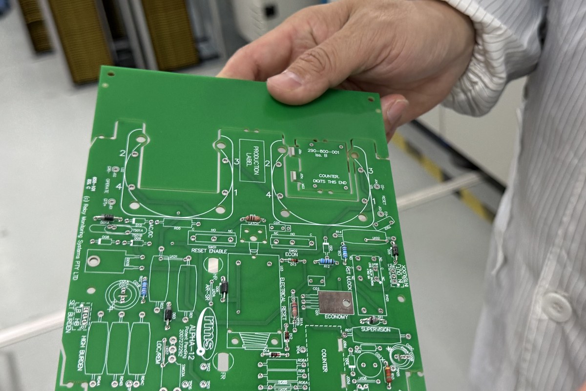
Do not copy a universal trace/space table into the drawing
Minimum geometry depends on finished copper, layer type, copper distribution, board construction and the specific fabrication process. A value that is routine on 1 oz copper may not be suitable on a much thicker layer.
Likewise, a manufacturing clearance is not automatically an adequate electrical insulation distance. High-voltage spacing must be selected from the product’s working voltage, transients, environment, applicable standard and coating or enclosure assumptions.
Acceptance should reference the agreed drawing and procurement requirements. IPC-6012F establishes qualification and performance requirements for rigid printed boards, while deviations and application-specific requirements must be stated in the procurement documentation.
Manufacturing sequence
From data review to finished-board acceptance
-
Review the build package
Check Gerbers or ODB++, drill data, stackup, finished copper by layer, materials, board thickness, tolerances, finish and acceptance notes.
-
Confirm the stackup and DFM rules
Resolve trace/space, resin fill, drill, annular-ring, copper-balance and panelization constraints before release.
-
Fabricate and control the board
Image and etch the conductive features, laminate the construction, drill and plate holes, apply finish and solder mask under the approved process route.
-
Inspect and test to the agreed scope
Use the required dimensional, visual, electrical and—when specified—coupon or microsection evidence against the released criteria.
-
Assemble under a thermal plan
If PCBA is ordered, develop the soldering and inspection route around the board’s thermal mass, component limits and test requirements.
What can increase cost or lead time?
- Higher or mixed copper weights
- Tight geometry relative to copper thickness
- Complex stackups or high layer count
- Deep resin-fill topography
- Small finished holes or demanding plating requirements
- Special materials, finishes or acceptance evidence
- Prototype thermal validation or assembly-profile development
Quote the actual construction
A meaningful price and schedule require the complete stackup and quantities. Generic “price per square inch” estimates can miss material, process and engineering requirements that dominate a heavy copper build.
If the board also needs components and testing, coordinate the bare-board release with our PCB assembly service rather than treating fabrication and PCBA as independent jobs.
Assembly and verification
Heavy copper PCB assembly needs a board-specific thermal plan
A larger copper mass can pull heat away from solder joints and create temperature differences across the assembly. That can affect paste behavior, wetting, through-hole soldering, component exposure and the time needed to reach the intended joint temperature.
Coordinate the layout and process before the first build
- Use thermal relief only where it meets the electrical and thermal objective.
- Review large copper-connected pads for solder balance and component float risk.
- Identify components with strict temperature or time-above-liquidus limits.
- Plan preheat, reflow or selective/hand-soldering steps for the actual board mass.
- Define inspection access and test coverage separately from bare-board electrical test.
SMT assembly planning covers paste printing, placement and reflow inputs. For higher-mix projects, the automated PCB assembly workflow explains how controlled build data supports repeatable setup and inspection.
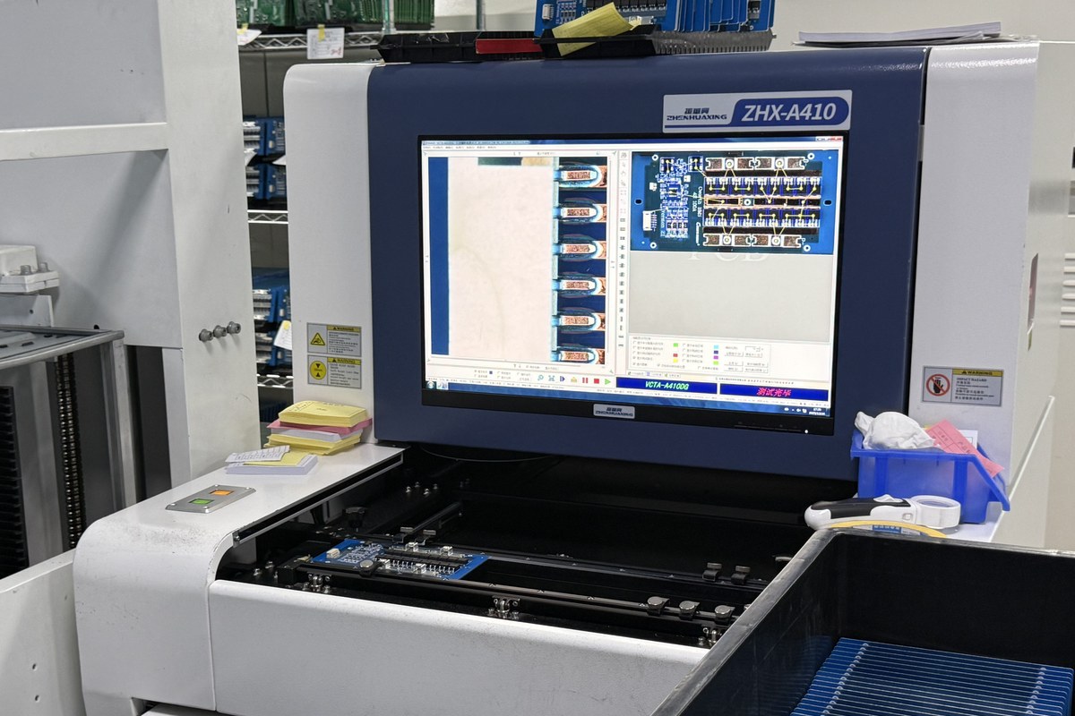
AOI can inspect defined visible assembly features, but it does not prove finished copper thickness, hidden joint integrity or product function. Use separate acceptance methods for the bare board, solder joints and functional requirements.
If your stackup and files are ready, send the heavy copper PCB package for DFM and quotation review. Include assembly data in the same submission when the order requires complete PCBA.
RFQ checklist
What to send for a heavy copper PCB quote
A controlled file set reduces clarification cycles and prevents copper, hole or assembly assumptions from becoming production requirements.
- Gerber or ODB++ data and drill files
- Layer stackup with finished copper per layer
- Material, board thickness and surface finish
- Fabrication drawing and dimensional tolerances
- Current, temperature and critical spacing notes
- Quantities, revision and requested delivery window
- BOM, CPL and assembly drawing for PCBA
- Electrical, inspection and test acceptance criteria
Mark any value that is a target rather than a mandatory limit. That gives engineering room to propose a manufacturable alternative without silently changing a critical requirement.
Start with one released revision
Name every file with the project and revision, and make sure the stackup, drawing, Gerbers and drill data describe the same board.
Request a heavy copper PCB review
The quotation and schedule are confirmed after engineering review of the complete data package.
Frequently asked questions
Heavy copper PCB FAQ
What qualifies as a heavy copper PCB?
There is no single universal commercial cutoff. Many buyers use heavy or thick copper for layers around 3 oz/ft² (about 105 µm) and above, while individual fabricators may use different definitions. State the required finished copper thickness for every layer instead of relying on the label alone.
Is heavy copper the same as a metal-core PCB?
No. Heavy copper describes thicker copper conductors on a PCB layer. A metal-core PCB uses a metal base or core as part of the construction. Either technology may support thermal management, but their stackups, insulation paths, fabrication rules and assembly behavior are different.
Can heavy copper carry more current?
A larger copper cross-section can support higher current or reduce conductor resistance, but copper weight alone does not establish a safe current rating. Trace width, layer position, ambient conditions, allowed temperature rise, nearby copper and cooling all affect the result.
Can heavy copper PCBs be assembled with SMT components?
Yes, when the board and assembly process are planned together. Higher copper mass can change heating and cooling behavior, so stencil design, thermal relief, pad balance, component limits, preheat and the validated soldering profile may need review.
What files are needed for a heavy copper PCB quote?
Send Gerber or ODB++ data, drill files, a layer stackup with finished copper per layer, material and thickness requirements, the fabrication drawing, quantities and acceptance criteria. Add the BOM, placement data, assembly drawing and test requirements if assembled boards are required.
Does a heavy copper PCB automatically solve thermal problems?
No. Thick copper can spread heat and reduce conductor resistance, but the complete thermal path still includes component interfaces, vias, dielectric materials, board area, enclosure conditions, airflow and any heat sink or chassis connection.
Related services
Continue planning the complete board build
When comparing a heavy copper PCB manufacturer, confirm finished copper by layer, achievable geometry, inspection coverage and the assembly thermal plan against the same released revision. A thick copper PCB quotation should state which fabrication and assembly operations are included, especially for power electronics and high-mix variants.
OrinewPCB coordinates one-stop PCB assembly for small-to-medium and high-mix builds, with 100% new and original components. Its nine-step quality and test workflow is applied through a project-defined inspection and acceptance plan. Manufacturer and distributor relationships support BOM pricing and supply planning; the earliest practical delivery is confirmed after material availability and test preparation are reviewed.
Use these pages to coordinate fabrication, assembly and controlled release data around the same PCB revision.