Power Bank PCB Manufacturing & Assembly
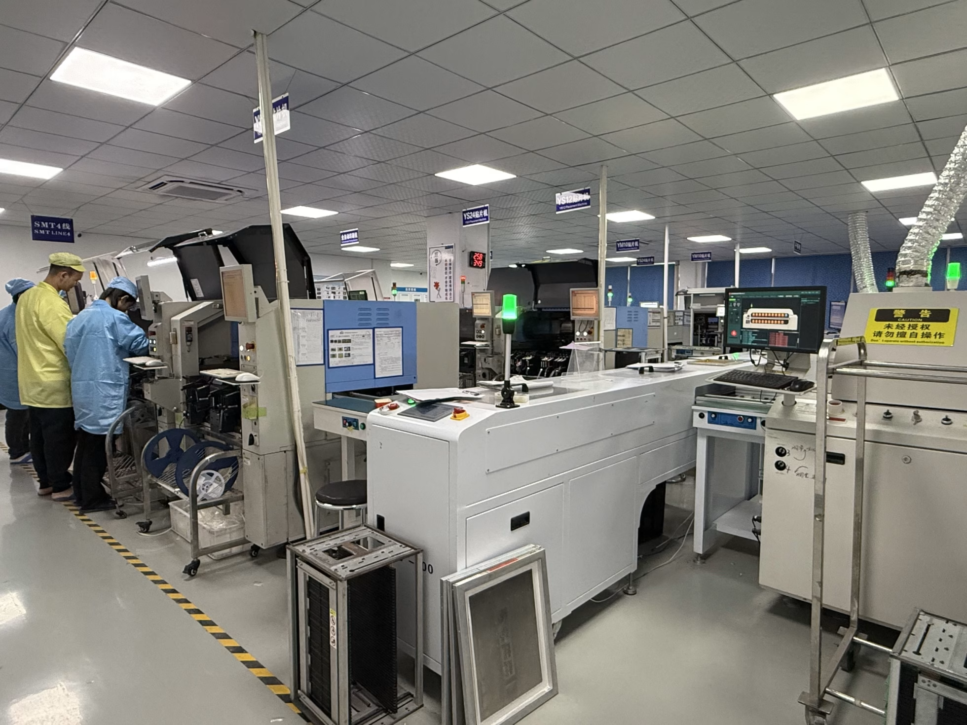
OrinewPCB provides custom power bank PCB manufacturing and assembly for OEM charger programs. We coordinate DFM, board fabrication, 100% new and original components, assembly, programming and project-defined testing, with material and delivery planning for small-to-medium, high-mix builds.
14+
Years Experience
98.15%
On-Time Delivery
96%
customer satisfaction rate
99%
Quality Pass Rate
Custom power-path, charging and interface PCBA planned as one controlled product revision
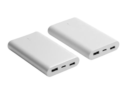
A power bank PCB is the control and power-conversion circuit board inside a portable battery product. Depending on the design, the power bank circuit board may manage cell charging, protection, boost or buck-boost conversion, USB input and output negotiation, state-of-charge indication, temperature sensing and user controls. A custom board should therefore be defined by the battery configuration, input and output profiles, target power, connector set, enclosure, thermal limits, firmware and required safety evidence—not by copying an off-the-shelf module.
OrinewPCB can review a custom PCB for a power bank and coordinate board fabrication with 100% new and original ICs and components, SMT/THT assembly, programming and project-specific testing. This one-stop PCB assembly route is most useful for prototypes, small-to-medium batches and multiple product variants because the PCB revision, charger and protection ICs, connector footprints, BOM alternatives and test limits stay connected. Battery cells, enclosure integration and finished-product certification are included only when they are explicitly reviewed and confirmed in the quotation scope.
Choose the board route from the actual application
The simplest suitable construction is usually easier to control than a more complex board selected from an application label. The following comparison turns the product requirement into a release decision.
| Route | Use it when | Release decision |
|---|---|---|
| Off-the-shelf power bank module | A development fixture or simple internal prototype can use an existing module without a custom form factor | Verify ratings, documentation and whether the module is suitable for the intended product |
| Custom power bank PCB | Mechanical layout, connectors, indicators, firmware or power performance require a dedicated board | Release schematic, PCB data, BOM, enclosure and electrical requirements |
| Custom power bank PCBA | The project needs assembled and tested boards rather than bare PCBs | Add CPL, assembly drawing, programming and functional-test definition |
| Finished portable-power product | Cells, enclosure, cables, labels and market compliance are part of the deliverable | Define the wider product, certification and responsibility boundary separately |
Power Bank PCB Manufacturing and Assembly: design and DFM controls
A useful DFM review focuses on the electrical, thermal, mechanical and sourcing facts that can change fabrication or assembly. It should not rely on a generic capability list.
Define the complete power path
State cell arrangement, input sources, output ports, continuous and peak current, charging limits, conversion topology and protection concept. These inputs drive copper, vias, component selection and heat.
Select controller ICs by function and availability
Charger, protection, fuel-gauge and USB-PD devices should be identified by exact MPN and approved alternates. A pin-compatible part may still change firmware, thresholds or thermal behavior.
Coordinate board and enclosure geometry
USB connectors, buttons, displays, light pipes, cell tabs, mounting holes and cable exits must match the enclosure model and mechanical datum scheme.
Review heat sources and copper spreading
Inductors, switching MOSFETs, charging ICs, current-sense elements and connectors can dominate temperature rise. Use copper area, vias and airflow assumptions that match the installed product.
Keep battery safety responsibilities explicit
The PCBA can implement protection functions, but cell selection, pack construction, insulation, mechanical abuse and finished-product certification require their own verified controls.
How the manufacturing and assembly route is controlled
A reliable build connects product requirements, PCB data, component identity, assembly instructions and acceptance evidence. Each gate below should close against one released revision.
- Electrical scope: Confirm cell configuration, ports, charging and output profiles, power limits and protection functions.
- PCB and mechanical review: Align board outline, copper, thermal design, connectors, indicators and enclosure clearances.
- BOM risk review: Confirm authentic components, approved alternates, firmware dependencies and long-lead power ICs.
- Fabrication and assembly: Build the released PCB and apply the planned SMT/THT, connector and programming sequence.
- Controlled power-up: Use current limits, known loads and customer-approved test steps to verify rails and basic behavior.
- Functional release: Record the agreed charging, output, indicator, protection and programming results for the correct revision.
Files to send for an engineering review
Complete inputs shorten clarification time and prevent assumptions from becoming purchasing or production commitments. Every file should carry the same board, BOM and variant revision.
| Input | Required detail | Decision supported |
|---|---|---|
| PCB package | Gerber/ODB++, drill, outline, stackup, copper and fabrication notes | Bare-board manufacture and DFM |
| Assembly package | BOM with MPNs, CPL, drawings, polarity, variants and substitution rules | Sourcing and placement |
| Power definition | Cell arrangement, input/output profiles, continuous and peak current, efficiency or thermal goals | Power-stage and copper review |
| Mechanical inputs | Enclosure model or drawing, connector datum, buttons, display, cell tabs and mounting | Fit and interface alignment |
| Firmware and test | Programming file, version, fixtures, loads, limits and pass/fail criteria | Controlled power-up and functional test |
| Commercial inputs | Prototype/lot quantities, variant mix, target date and required records | Quotation and delivery plan |
When the package is ready, send the PCB files, BOM, quantities and acceptance requirements for a combined engineering review. OrinewPCB can identify open construction, sourcing, assembly and test questions before confirming the quotation scope.
One-stop component sourcing and PCB assembly
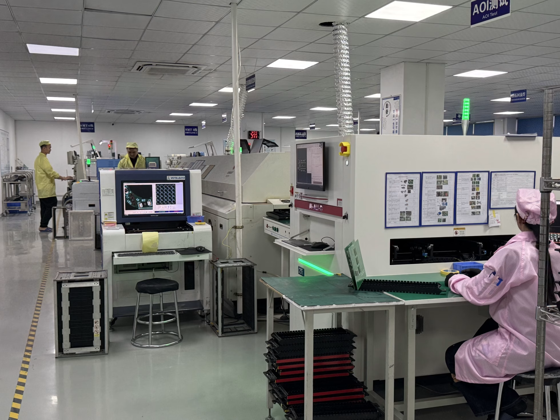
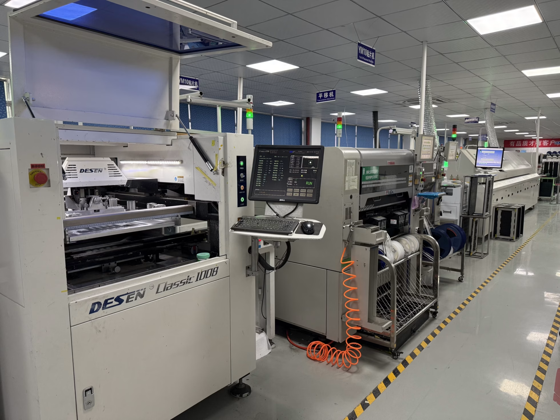
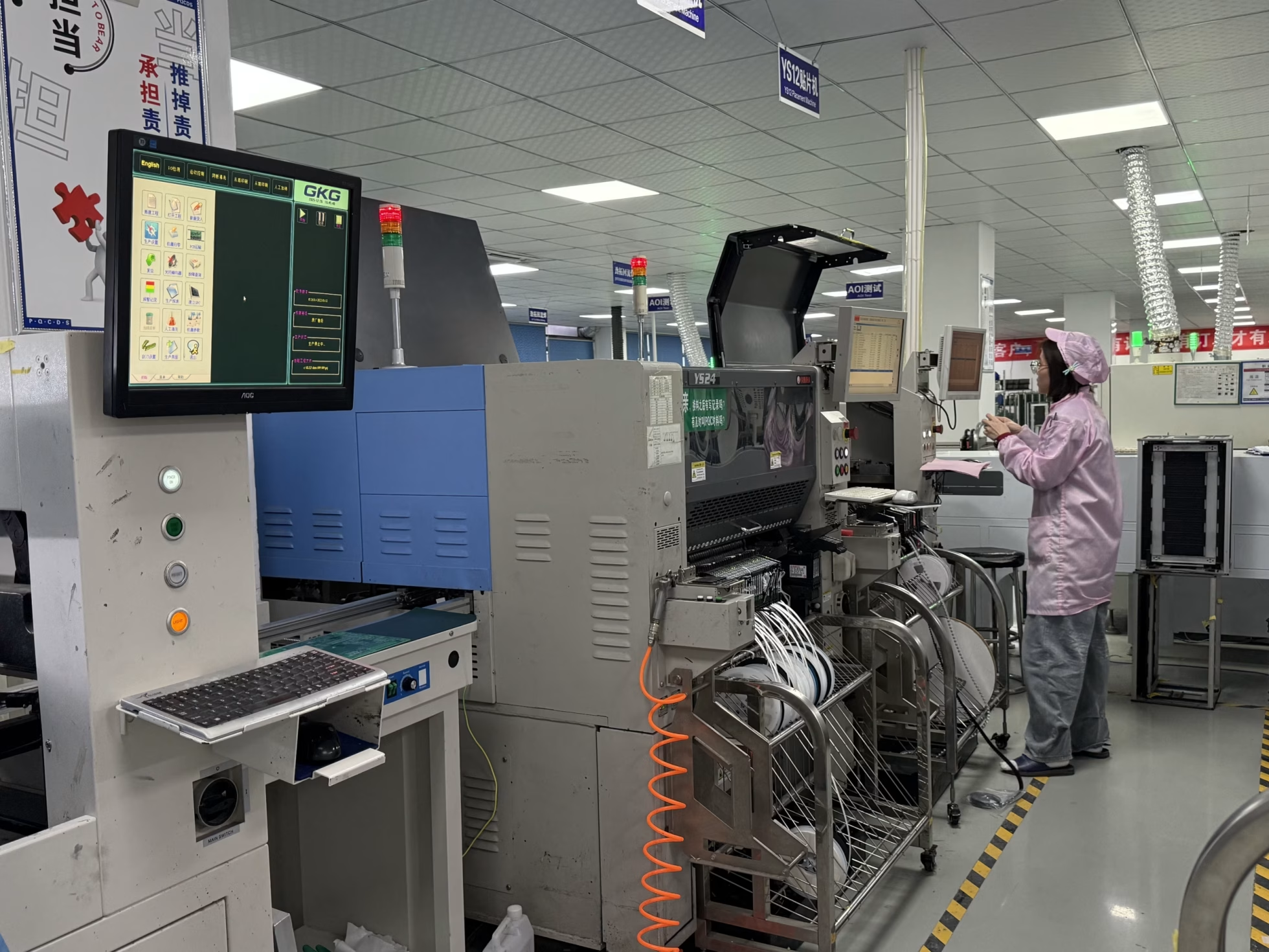
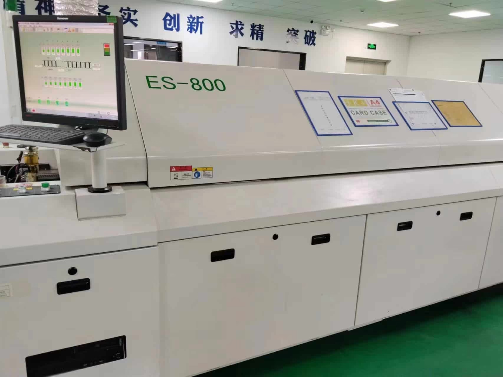
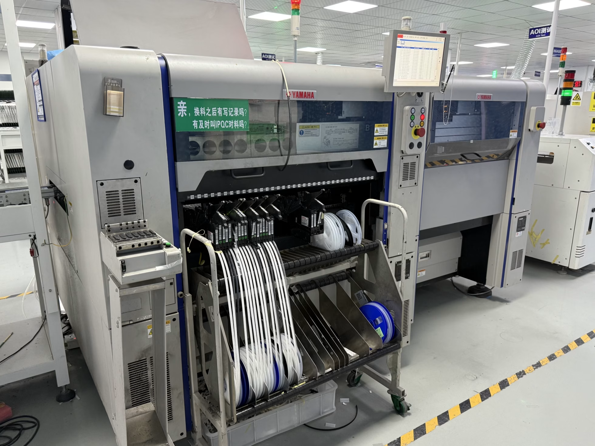
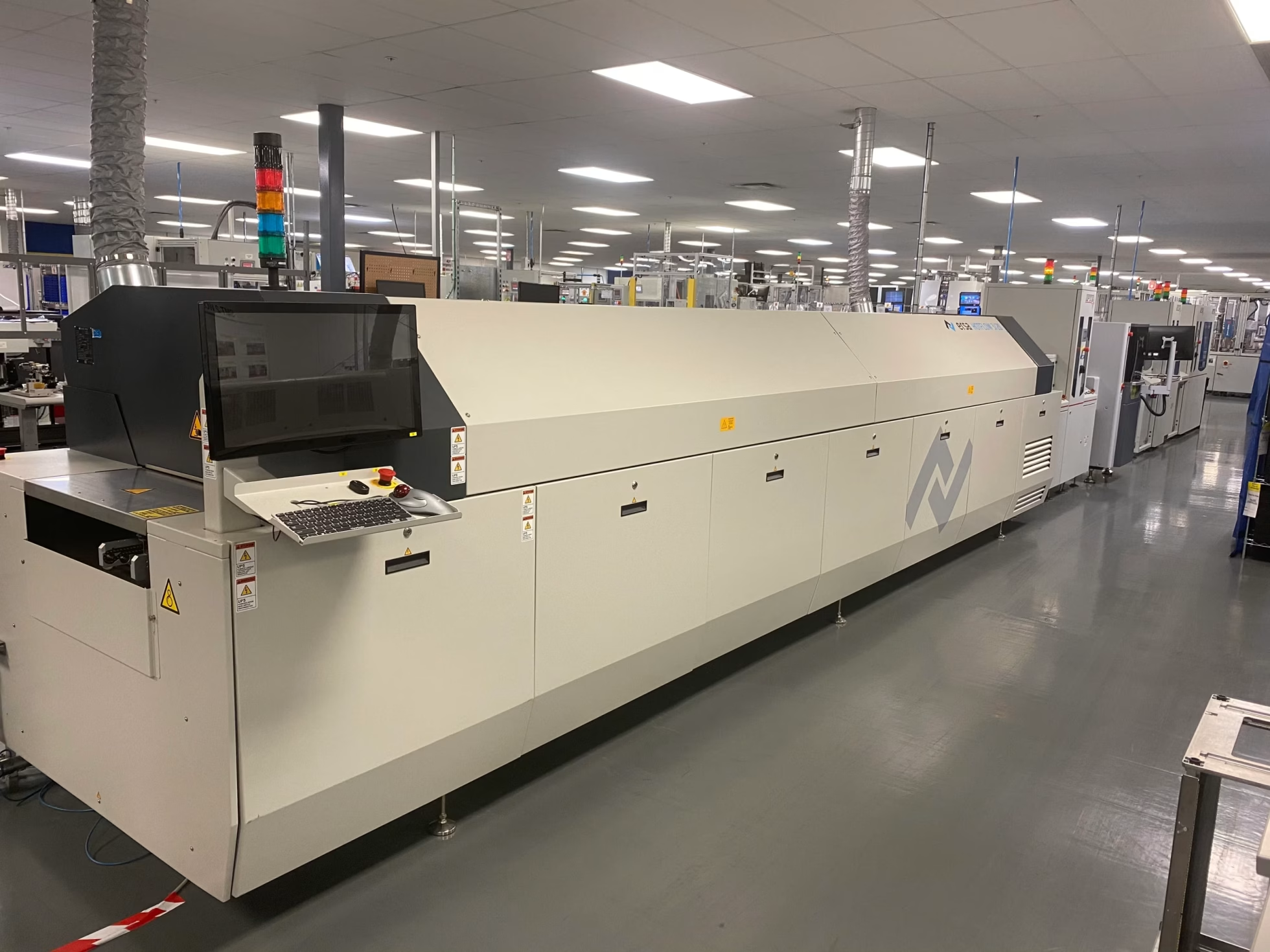
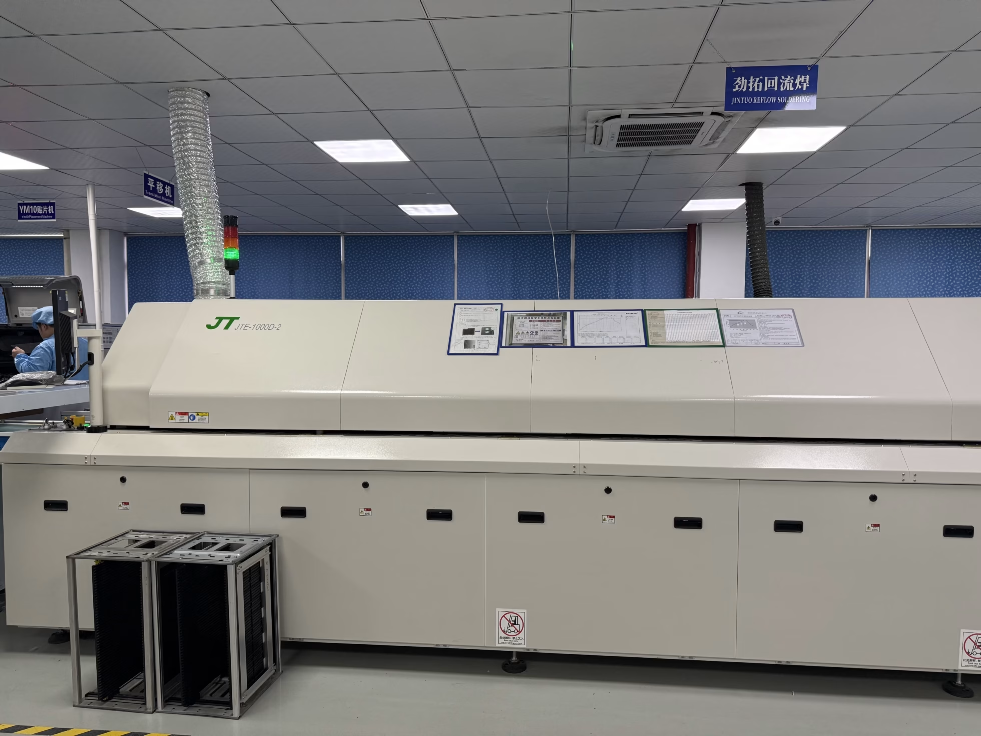
Power bank PCB assembly combines fine-pitch control ICs, power devices, inductors, connectors and sometimes mixed SMT/THT operations. The assembly plan should address solder-paste volume, thermal mass, connector coplanarity, polarity, programming access and safe power-up. The custom PCB assembly service supports product-specific fixtures and variants, while turnkey PCB assembly keeps original component sourcing and the agreed test scope with the board build.
Review heavy-copper PCB planning when current and temperature rise drive the construction, and use the main PCB manufacturing service for fabrication inputs and board options.
Quality and test planning must match the released product
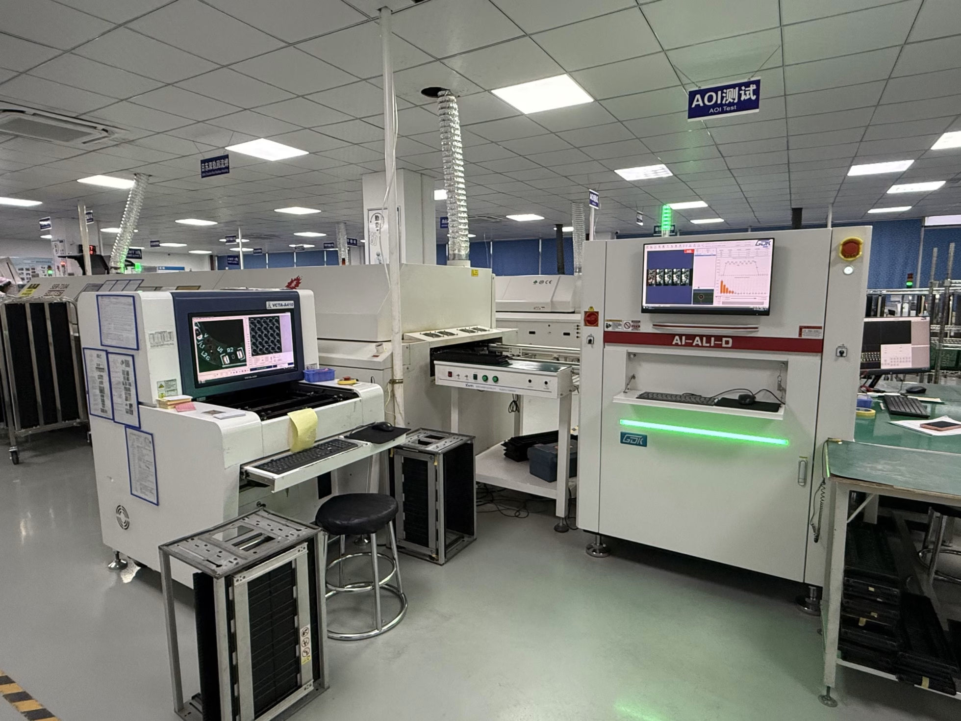
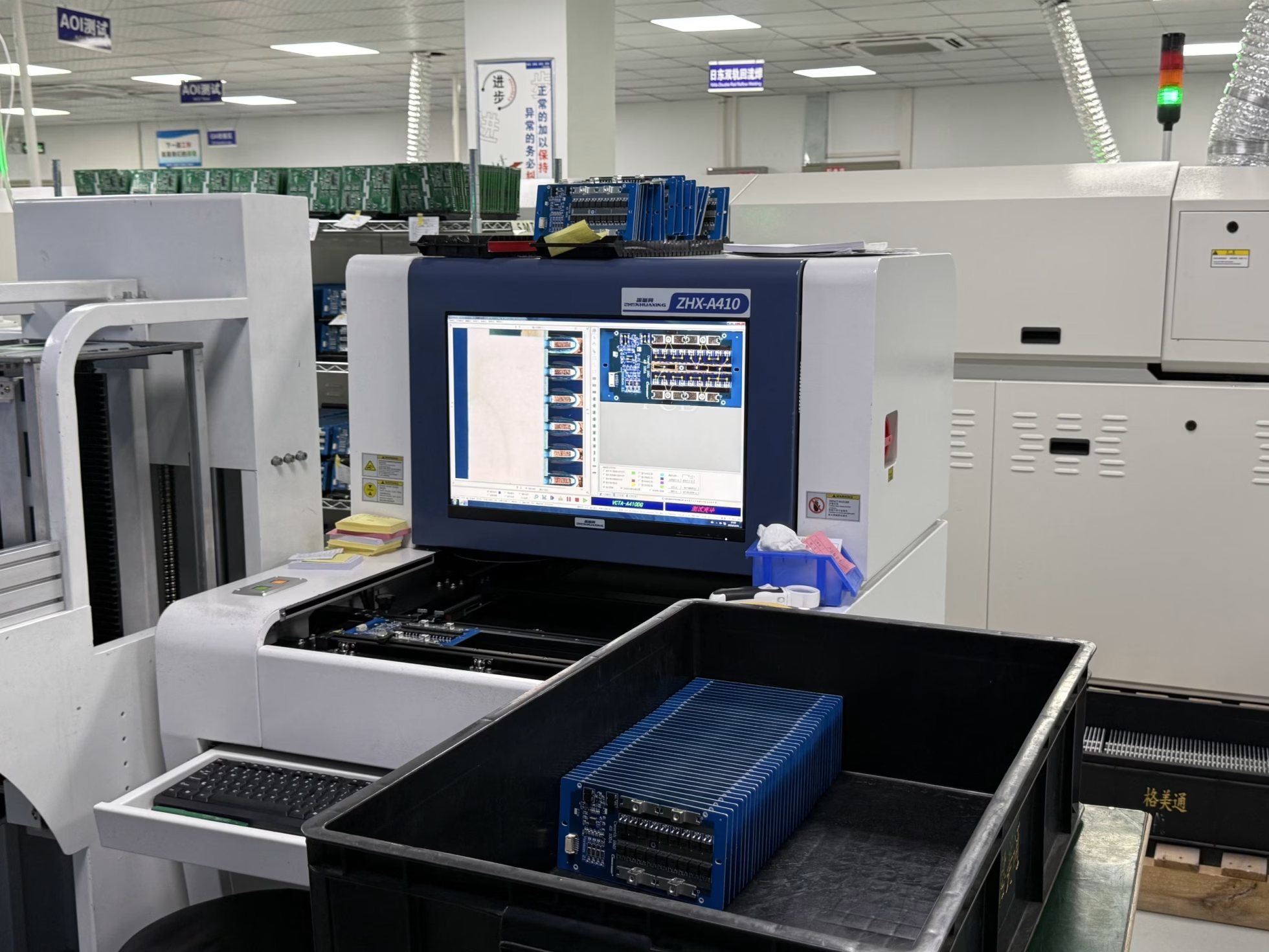
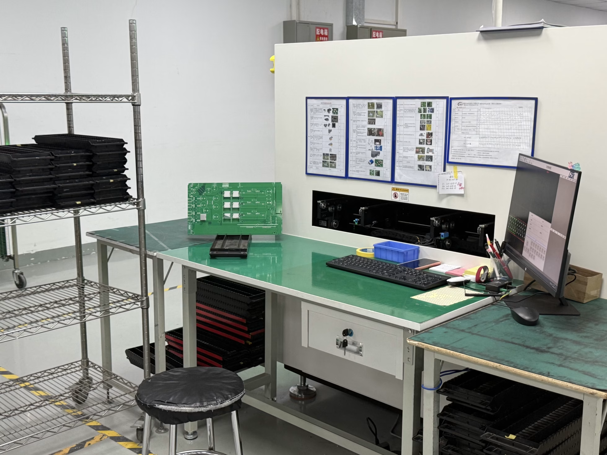
OrinewPCB uses a nine-step quality and test workflow, but the meaningful acceptance plan for a power bank PCBA must be written around the product. It may include incoming component checks, solder-paste and placement controls, AOI, polarity inspection, controlled power-up, programming, charging and output checks, indicator behavior and customer-defined protection tests. Destructive battery abuse, certification and pack-level validation are not implied unless explicitly included in the approved scope.
- Resolve conflicting PCB, BOM, placement and drawing revisions before materials are committed.
- Record approved component alternates and the engineering conditions attached to each substitution.
- Define the inspection, programming and functional evidence that will be delivered with the build.
- Return accepted deviations and rework findings to the next controlled release.
Cost and lead-time factors
Power bank PCB cost and lead time depend on layer count, copper and thermal needs, connectors, power IC availability, approved alternates, programming, fixtures and functional-test depth. A low-cost off-the-shelf module may dominate generic search results, but it is not the same buying decision as a custom OEM power bank PCB. Early review of the exact MPNs and enclosure interfaces helps avoid redesign after components or tooling are committed.
OrinewPCB works with manufacturers and authorized or established distribution channels to support component pricing and material schedules, while maintaining the stated requirement for 100% new and original parts. Delivery is planned for the earliest practical date after construction, material, assembly and test inputs are confirmed.
Power Bank PCB FAQ
What is a power bank PCB?
It is the circuit board that manages charging, protection, power conversion, USB interfaces, indicators and controls in a portable battery product, according to the specific design.
Is a custom power bank circuit board different from a retail module?
Yes. A custom board is designed around the released electrical, mechanical, firmware and product requirements; a retail module is a pre-defined product with its own ratings and documentation.
What files are needed for a power bank PCB assembly quote?
Provide PCB fabrication data, BOM with MPNs, placement and assembly files, cell and power requirements, enclosure information, quantities, programming data and test criteria.
Can OrinewPCB source the power-management components?
OrinewPCB can source 100% new and original components within the approved PCBA scope. Exact MPNs, alternates and firmware dependencies should be confirmed before purchasing.
Plan the next build from one controlled data set
The PCB construction, component BOM, placement revision, product interfaces and acceptance criteria should describe the same deliverable. That alignment is especially important for prototypes, small-to-medium batches and high-mix programs where several variants may share similar files.
If the design is ready for review, provide the released manufacturing data and project requirements for the next-build assessment. The returned scope can address PCB fabrication, original component sourcing, assembly, project-defined testing and the earliest practical delivery plan together.
The Benefits of Partnering with OrinewPCB as Your OEM Power Bank PCB Board Assembly Suppliers
For a custom OEM power bank PCB assembly, the useful supplier benefits are controlled files, approved component identity, assembly planning and a written test scope. The following items must be confirmed for the actual project:
- Tailored designs to meet specific power bank requirements
- Flexibility in component selection and board layout
- Efficient production processes to reduce overall costs
- Bulk ordering options for better pricing
- Project-defined inspection and functional checks
- Applicable safety and performance requirements must be supplied and confirmed in the approved scope
- Expert guidance throughout the design and production phases
- Ongoing assistance for product improvements and updates
PCB Factory Gallery