
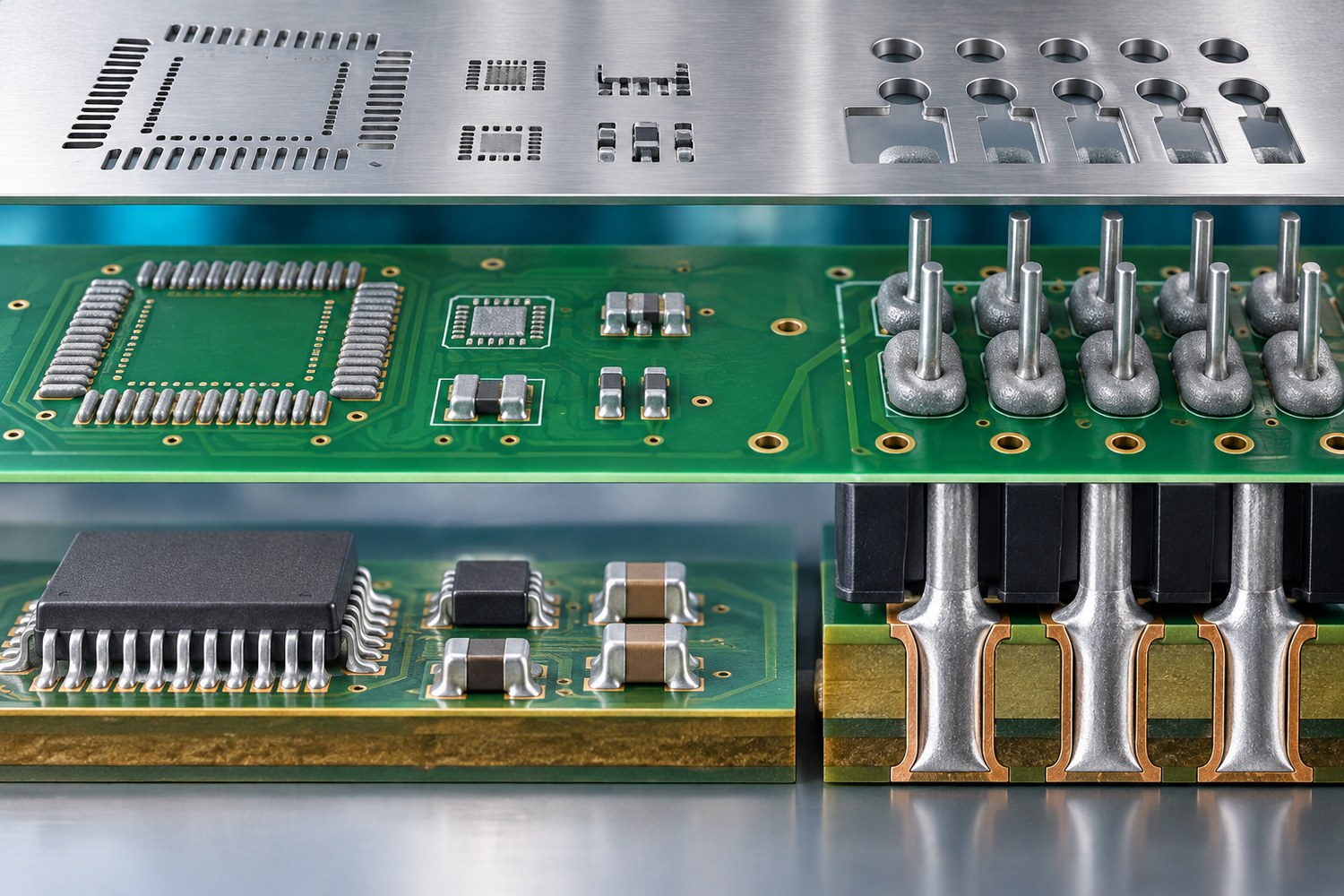

Solder-paste transfer design connected to the PCB, component and reflow process
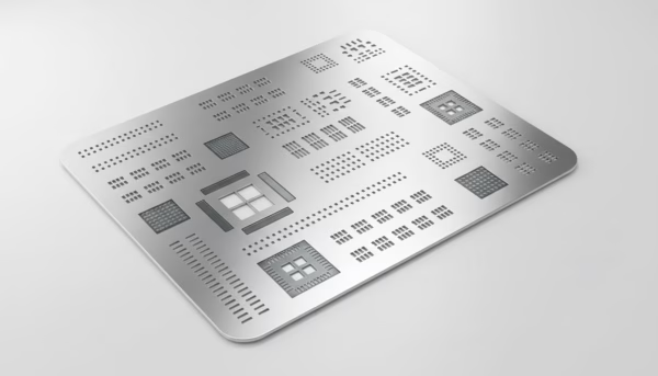
An SMT stencil is a patterned metal foil used to deposit solder paste onto PCB pads before surface-mount placement. Stencil performance depends on more than foil thickness: aperture geometry, reduction, area ratio, step regions, board support, printer settings, paste and component termination all influence transfer. A PCB stencil should therefore be released from the same paste-layer revision as the board and reviewed against the package mix and reflow process.
OrinewPCB can coordinate the solder-paste stencil with PCB fabrication, 100% new and original component sourcing, SMT assembly and the nine-step quality and test workflow. For small-to-medium batches and high-mix products, keeping stencil revision, PCB revision and component package data together reduces the risk of using an aperture design that belongs to an earlier BOM or footprint set.
When should you choose SMT Stencil?
The correct route is the simplest construction that satisfies the released electrical, mechanical, thermal, compliance and assembly requirements. Use the comparison below to define why this board type is necessary before specifying details.
| Route | Use it when | Release decision |
|---|---|---|
| Frameless stencil | Prototype or manual/semi-automatic printing with a compatible holder | Confirm frame system, handling and alignment |
| Framed laser-cut stencil | Repeatable production printing on a defined printer | Specify frame, foil, tension and usable image area |
| Step stencil | Fine-pitch and high-volume deposits need different paste volumes | Review step location, transition and squeegee travel |
| Nano-coated stencil | Release behavior or cleaning interval justifies the coating | Validate with paste, aperture mix and production evidence |
SMT Stencil design and DFM controls
The most useful DFM review checks the features that control fabrication and assembly risk, rather than comparing the design with a generic capability list.
Start from the released paste layer
Do not recreate apertures from a screenshot or an obsolete Gerber export. Match the stencil to the exact PCB and BOM revision.
Review area ratio and aperture shape
Small apertures may not release paste consistently even when they match the copper pad. Package-specific reductions or shapes may be required.
Balance paste volume across packages
Fine-pitch ICs and large thermal or pin-in-paste joints can require different deposit volumes and may justify a step stencil.
Plan printer support and fiducials
Board support, underside clearances, fiducials, frame and squeegee direction affect print alignment and repeatability.
How the manufacturing route is reviewed
A reliable build keeps the requirement, material, fabrication data and acceptance evidence connected through the release process. The exact operations vary with construction, but the following gates should be explicit.
- Data reconciliation: Align PCB paste layer, component packages, BOM and assembly drawing.
- Aperture review: Evaluate reductions, shapes, home-plate features and special deposits.
- Foil and frame selection: Choose thickness, frame system and any step or coating requirement.
- Laser cutting and finishing: Create and finish apertures for the approved design.
- Printing setup: Set support, alignment, paste, pressure, speed and cleaning plan.
- First-article feedback: Use print and solder evidence to control any approved stencil revision.
Files to send for an engineering review
Every file should identify the same board revision. A complete package shortens clarification time and makes price, material and delivery assumptions visible before production.
| Input | Required detail | Decision supported |
|---|---|---|
| Fabrication data | Gerber, ODB++ or IPC-2581 plus NC drill and board outline | Layer interpretation, holes, profile and DFM review |
| Stackup and materials | Layer order, finished thickness, copper, material and approved-equivalent rules | Construction and material proposal |
| Special requirements | Impedance, mechanical, compliance, finish, marking or documentation needs | Process selection and quotation scope |
| Assembly package | BOM, CPL, assembly drawing, variants and substitution rules when PCBA is required | Original-part sourcing and assembly planning |
| Test and delivery | Acceptance method, required evidence, quantity and target delivery | Inspection, test and schedule basis |
When the release package is ready, share the fabrication files and assembly inputs for a combined engineering review. OrinewPCB can then identify open DFM, material, sourcing and test questions before confirming the quotation scope.
SMT Stencil in one-stop PCB assembly
The stencil is part of the SMT process, not an isolated accessory. A technically correct stencil can still produce poor deposits when board support, paste condition, printer settings or cleaning are uncontrolled. The SMT assembly service connects stencil design with printing, placement, reflow and inspection evidence.
Review the prototype PCB assembly route for first-article validation, the turnkey PCB assembly scope for complete sourcing and production, and the parent PCB manufacturing service for the fabricated-board inputs.
Quality, cost and lead-time factors
OrinewPCB uses a nine-step quality and test control framework that links release review, materials, fabrication, assembly and final verification. The actual inspection and test methods are selected for the board and customer-defined acceptance scope; not every board needs every method.
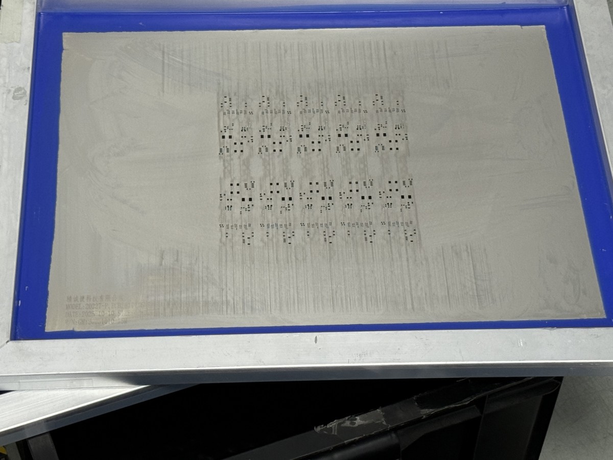
SMT stencil cost and delivery depend on foil size and thickness, frame, aperture count, step regions, coating, electropolishing and revision frequency. The more important cost is often production impact: an incorrect stencil can create rework, insufficient solder or bridging across an entire lot.
- Resolve missing or conflicting data before material is committed.
- Keep approved substitutions and evidence requirements in the released order.
- Confirm panel, tooling and assembly constraints together when PCBA is included.
- Plan delivery as early as practical after material, process and test inputs are reviewed.
SMT Stencil FAQ
What is an SMT stencil?
It is a patterned foil that transfers solder paste onto PCB pads before surface-mount components are placed.
How is stencil thickness selected?
Thickness is selected against the package and aperture mix, required paste volume, area ratio, step needs and printing process.
When is a step stencil useful?
A step stencil can be useful when fine-pitch apertures and larger thermal, connector or pin-in-paste deposits require different paste volumes.
What files are needed for a PCB stencil?
Provide the released paste layer, PCB outline, fiducials, panel data, component package information, printer or frame requirement and any special aperture instructions.
Plan the next build from one controlled data set
The board construction, component BOM, assembly revision and acceptance plan should describe the same product. This reduces supplier handoffs and makes engineering decisions easier to trace across prototypes, small-to-medium batches and high-mix production.
If the project is ready to move forward, provide the released PCB data, BOM, quantities and test requirements for the next-build review. The returned scope can address fabrication, 100% new and original component sourcing, assembly, testing and the earliest practical delivery plan together.