
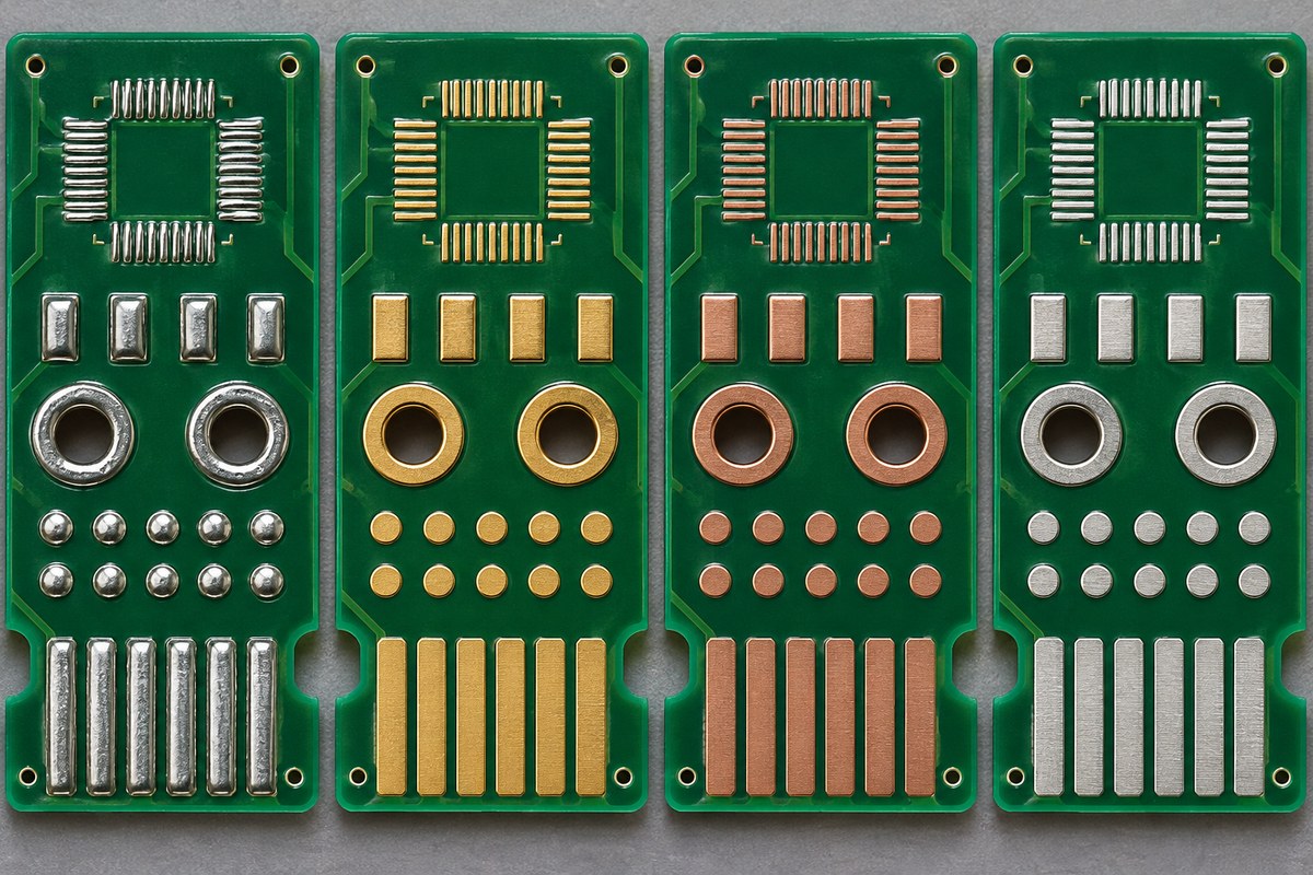

Conventional rigid-board fabrication with a controlled release package
Standard PCB manufacturing is the practical route for conventional rigid printed circuit boards when the design does not require a specialized flex, RF, heavy-copper or sequential-build structure. The term usually covers common single-layer, double-sided and multilayer constructions, but it is not a substitute for a fabrication drawing. Material family, layer count, finished thickness, copper weight, surface finish, hole definition, impedance needs and acceptance requirements still have to be stated for each order.
OrinewPCB reviews the released PCB data before confirming a manufacturing route. If the project also needs components and assembly, the same controlled revision can continue into one-stop PCB assembly with 100% new and original component sourcing, assembly and project-specific testing. This is especially useful for small-to-medium batches and multiple board variants because fabrication, BOM and assembly decisions stay connected.
When should you choose Standard PCB?
The correct route is the simplest construction that satisfies the released electrical, mechanical, thermal, compliance and assembly requirements. Use the comparison below to define why this board type is necessary before specifying details.
| Route | Use it when | Release decision |
|---|---|---|
| Standard rigid PCB | Conventional FR-4-based board with common drilling and finish requirements | Layer stack, copper, thickness, finish and test requirements |
| Double-sided PCB | Routing and interconnection are needed on both sides without a multilayer stack | Plated holes, component side, soldering route and panel plan |
| Four-layer or multilayer PCB | Power planes, routing density or EMC needs exceed two layers | Stack order, reference planes, copper balance and impedance |
| Specialized PCB route | Flexing, RF loss, high thermal load or high current changes the construction | Use a dedicated flex, high-frequency, high-Tg or heavy-copper review |
Standard PCB design and DFM controls
The most useful DFM review checks the features that control fabrication and assembly risk, rather than comparing the design with a generic capability list.
Define construction, not only layer count
A layer count does not identify dielectric thickness, finished board thickness, copper weight or reference-plane relationships. Put these requirements in the fabrication package.
Control holes and edge features
Separate plated and non-plated holes, dimension slots and cutouts, and identify castellations, edge plating or countersinks when they are required.
Select the finish with assembly in mind
Pad flatness, shelf life, soldering process and contact use influence whether HASL, ENIG, OSP or another finish is appropriate.
Align the panel with assembly
Rails, tooling holes, fiducials and breakaway methods affect both bare-board yield and downstream SMT handling.
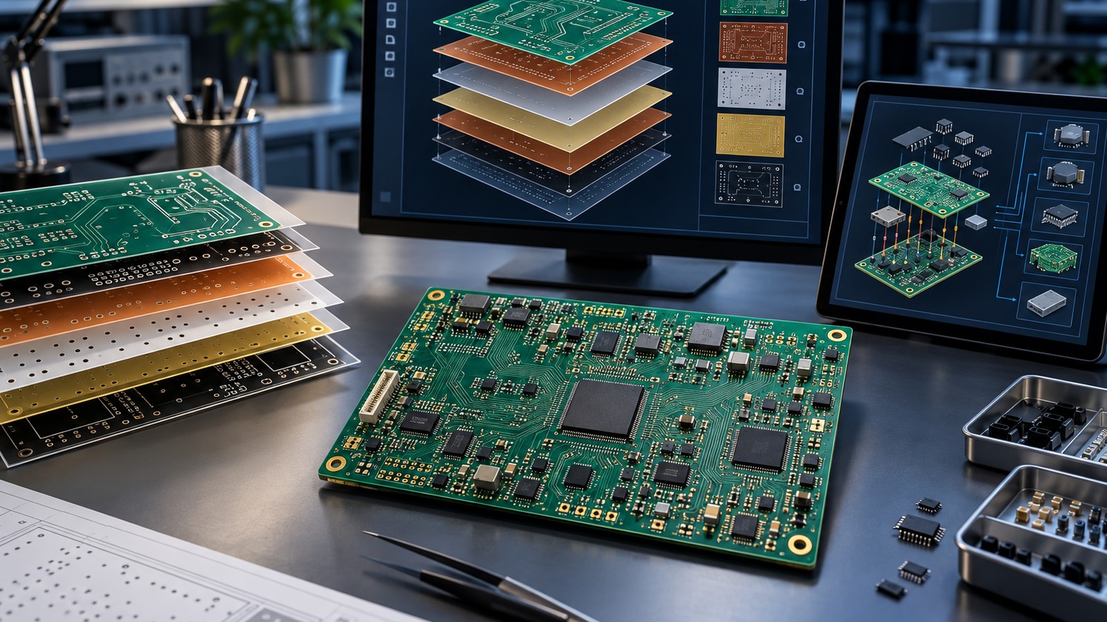
How the manufacturing route is reviewed
A reliable build keeps the requirement, material, fabrication data and acceptance evidence connected through the release process. The exact operations vary with construction, but the following gates should be explicit.
- Release review: Confirm that Gerber or ODB++, drill, outline and notes describe one revision.
- Stack and material review: Resolve copper weight, dielectric, thickness and controlled-impedance inputs.
- Imaging and lamination: Pattern copper layers and laminate the approved multilayer construction when applicable.
- Drilling and plating: Create the released hole pattern and conductive interconnections.
- Mask, legend and finish: Apply the specified solder mask, marking and surface finish.
- Electrical and final checks: Apply the agreed bare-board test, visual checks and release records.
Files to send for an engineering review
Every file should identify the same board revision. A complete package shortens clarification time and makes price, material and delivery assumptions visible before production.
| Input | Required detail | Decision supported |
|---|---|---|
| Fabrication data | Gerber, ODB++ or IPC-2581 plus NC drill and board outline | Layer interpretation, holes, profile and DFM review |
| Stackup and materials | Layer order, finished thickness, copper, material and approved-equivalent rules | Construction and material proposal |
| Special requirements | Impedance, mechanical, compliance, finish, marking or documentation needs | Process selection and quotation scope |
| Assembly package | BOM, CPL, assembly drawing, variants and substitution rules when PCBA is required | Original-part sourcing and assembly planning |
| Test and delivery | Acceptance method, required evidence, quantity and target delivery | Inspection, test and schedule basis |
When the release package is ready, share the fabrication files and assembly inputs for a combined engineering review. OrinewPCB can then identify open DFM, material, sourcing and test questions before confirming the quotation scope.
Standard PCB in one-stop PCB assembly
A standard printed circuit board may be straightforward to fabricate, yet assembly can still fail when footprints, component packages, panel rails or finish choices are not coordinated. The board package should be reviewed with the BOM, CPL and assembly drawing before the order is released. For a complete build, the turnkey PCB assembly workflow keeps the fabricated board, original components, placement data and agreed test scope under one project revision.
For related construction decisions, compare the FR-4 PCB material route, the four-layer PCB stackup and the broader PCB manufacturing service.
Quality, cost and lead-time factors
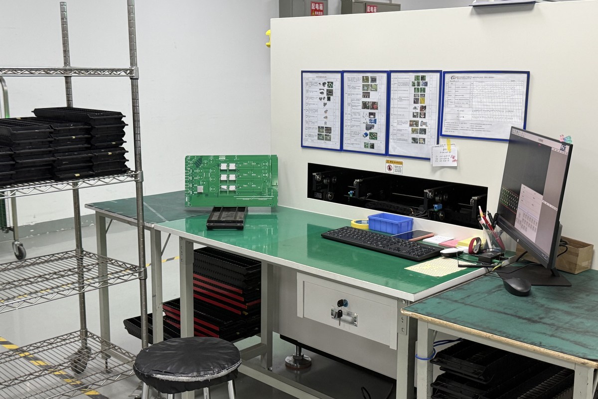
OrinewPCB uses a nine-step quality and test control framework that links release review, materials, fabrication, assembly and final verification. The actual inspection and test methods are selected for the board and customer-defined acceptance scope; not every board needs every method.
Cost is driven by board area, panel utilization, layer count, copper weight, drill count, minimum geometry, finish, quantity and the required records. A common material name alone does not guarantee the lowest total cost; a manufacturable panel and a stable assembly release can matter more than a small laminate price difference.
- Resolve missing or conflicting data before material is committed.
- Keep approved substitutions and evidence requirements in the released order.
- Confirm panel, tooling and assembly constraints together when PCBA is included.
- Plan delivery as early as practical after material, process and test inputs are reviewed.
Standard PCB FAQ
What is a standard PCB?
A standard PCB is a conventional rigid printed circuit board that does not require a specialized flex, RF, heavy-copper or sequential-build construction. Its actual material, stackup and acceptance requirements still need to be specified.
What files are needed for standard PCB fabrication?
Send Gerber, ODB++ or IPC-2581 data, NC drill files, board outline, stackup notes, quantity, finish and any impedance or acceptance requirements.
Can standard PCBs be supplied as assembled boards?
Yes. The fabrication package can continue into component sourcing, SMT or through-hole assembly and the agreed inspection or test scope.
What determines standard PCB lead time?
Construction, material availability, panel use, drill and finish requirements, quantity and open engineering questions determine the practical schedule.
Plan the next build from one controlled data set
The board construction, component BOM, assembly revision and acceptance plan should describe the same product. This reduces supplier handoffs and makes engineering decisions easier to trace across prototypes, small-to-medium batches and high-mix production.
If the project is ready to move forward, provide the released PCB data, BOM, quantities and test requirements for the next-build review. The returned scope can address fabrication, 100% new and original component sourcing, assembly, testing and the earliest practical delivery plan together.