
Arlon AD350A PCB: Material Properties, Applications, and Fabrication Notes
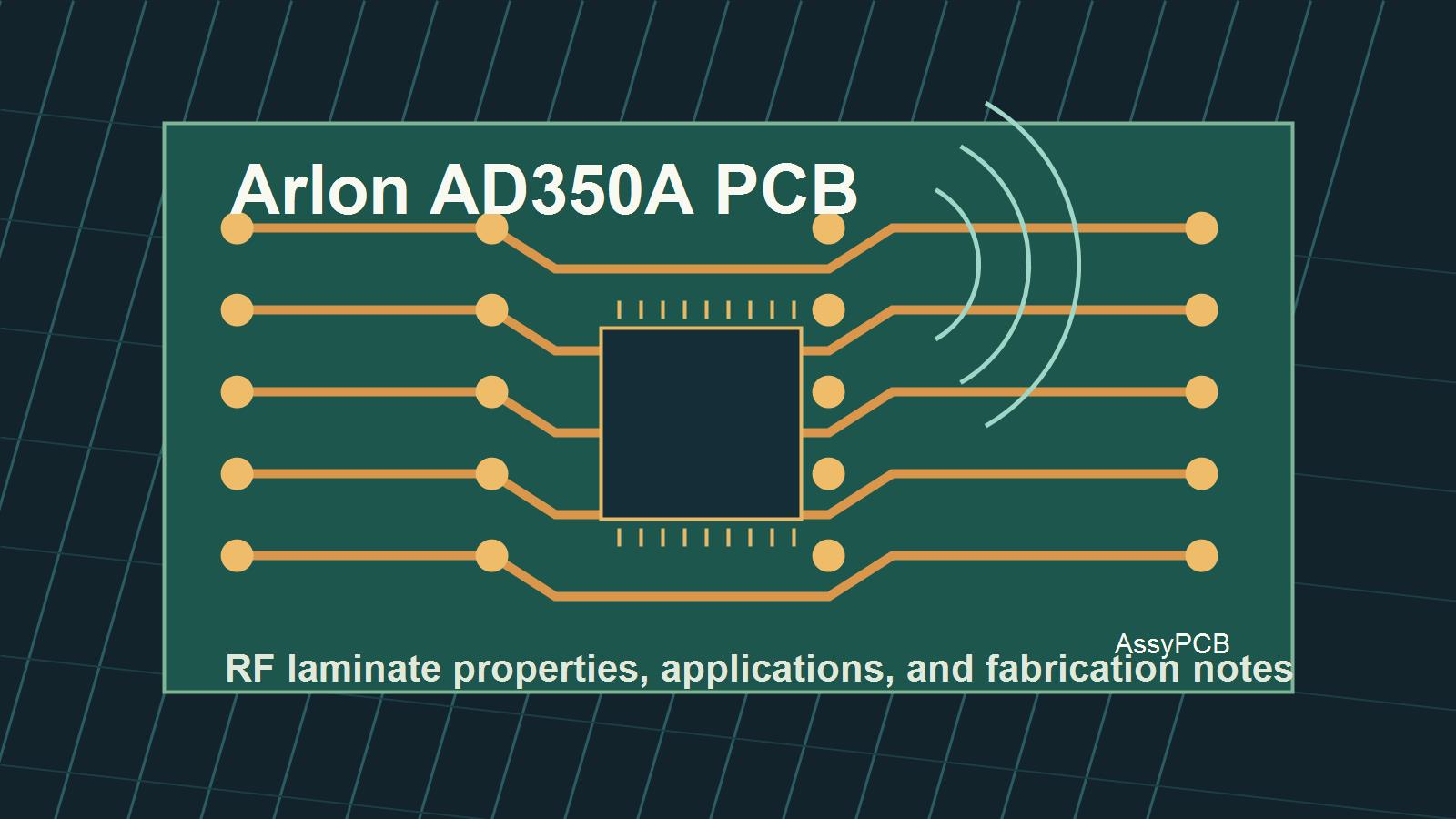
Table of Conent
Table of Conent
Arlon AD350A PCB material is a woven fiberglass reinforced, ceramic-filled, PTFE-based laminate from Rogers’ AD Series, designed for printed circuit board substrates that need controlled dielectric performance, low loss, and better heat handling than many general-purpose RF laminate choices.
If your design uses antennas, RF transmission paths, communications hardware, telematics, or higher-power RF sections, AD350A is worth a careful look. The important question is not whether the material is “premium.” The better question is whether its published electrical, thermal, and fabrication behavior matches your circuit, stackup, and manufacturing risk.
> Key Takeaways
> – AD350A is a PTFE, woven fiberglass, ceramic-filled PCB laminate with a process dielectric constant of 3.50 +/- 0.05.
> – Rogers lists the material with low insertion loss tangent of 0.003 at 10 GHz on the product page, while the property table lists typical dissipation factor as 0.0033 at 10 GHz.
> – The material is aimed at higher-power designs where heat rejection and lower thermal expansion matter.
> – AD350A is commonly relevant for antenna systems, antennas, communications systems, and telematics or infotainment designs.
> – A successful AD350A PCB build depends on laminate selection, stackup control, plated-through-hole reliability, copper roughness, drilling, and controlled impedance planning.
What Is Arlon AD350A PCB Material?
AD350A is part of Rogers’ AD Series laminates. Rogers describes the AD Series as PTFE/woven glass based laminates built for consistent high-frequency PCB performance in cost-sensitive commercial applications. Within that family, AD350A uses a woven fiberglass reinforced, ceramic-filled, PTFE-based composite structure.
That material construction matters because each part of the system does a job:
– PTFE supports low-loss high-frequency behavior.
– Woven fiberglass adds mechanical reinforcement.
– Ceramic filler helps tune dielectric and thermal properties.
– Copper foil and fabrication process control determine how the material performs as a finished PCB, not just as a datasheet line item.
For engineers, the practical point is simple: AD350A is not a drop-in replacement for standard FR-4. It belongs in the same conversation as other RF and microwave circuit materials, where dielectric constant, loss, thermal expansion, copper profile, and impedance tolerance all affect the final board.
If you are still at the material selection stage, it helps to review the broader requirements for a high frequency PCB before locking the stackup. The laminate is only one part of RF performance. Trace geometry, return paths, connector launch design, via transitions, and assembly quality all matter too.
Published AD350A Material Properties
The table below summarizes the public data Rogers lists for AD350A on its product page and AD Series property table. Use these values for early engineering comparison, then confirm the exact laminate thickness, copper type, and fabrication requirements before production.
| Property | Published AD350A Value | Why It Matters |
| Process dielectric constant | 3.50 +/- 0.05 | Helps predict impedance and phase behavior. |
| Design dielectric constant | 3.54 | Often used in practical circuit modeling. |
| Loss tangent / dissipation factor | 0.003 to 0.0033 at 10 GHz | Affects insertion loss in RF paths. |
| Z-axis thermal expansion | 35 ppm/C feature listing; 63 ppm/C typical table value from -55 C to 288 C | Important for plated-through-hole reliability and thermal cycling. |
| Thermal conductivity | 0.44 W/m/K typical at 50 C, ASTM D5470 | Supports heat spreading compared with lower-conductivity materials. |
| X/Y CTE | 18 ppm/C typical in both X and Y directions | Helps with dimensional stability. |
| Peel strength, 1 oz ED copper | 14.7 lb/in. typical, 2.6 N/mm | Relevant to copper adhesion and fabrication robustness. |
| Density | 2.43 g/cm3 typical | Useful for mechanical and weight estimates. |
| Flammability | UL94 V-0 | Supports compliance screening. |
| Lead-free process compatible | Yes | Important for modern assembly profiles. |
| Typical PIM | -164 dBc | Relevant for antenna and wireless designs where passive intermodulation matters. |
Two details deserve extra care. First, Rogers’ feature summary lists a low insertion loss tangent of 0.003 at 10 GHz, while the property table lists a typical dissipation factor of 0.0033 at 10 GHz. That is not unusual across summary and table formats, but your controlled documentation should specify which value was used in simulation and quotation.
Second, the Z-axis CTE appears in different contexts: the feature listing calls out 35 ppm/C, while the comparative property table lists 63 ppm/C over -55 C to 288 C. Do not mix these values casually. Thermal expansion depends on test method and temperature range, so production drawings should reference the manufacturer datasheet and the exact requirement.
Where AD350A PCB Makes Sense
AD350A is most relevant when a circuit needs RF-grade dielectric control and better thermal behavior than a generic low-cost laminate can provide. Rogers lists current applications including antenna systems, antennas, communications systems, and telematics and infotainment.
Typical use cases may include:
– RF antenna boards.
– Wireless infrastructure modules.
– Automotive telematics circuits.
– Communication system boards.
– Higher-power RF designs where heat rejection is part of the material decision.
– Designs where passive intermodulation performance needs attention.
Picture a telematics design where the RF section is compact, the enclosure runs warm, and the antenna feed geometry is sensitive to impedance drift. A standard FR-4 prototype may help prove digital logic, but it may not represent the RF behavior of the final product. In that situation, an AD350A prototype can give the engineering team a more realistic view of insertion loss, impedance control, and thermal behavior before committing to a larger build.
For a deeper background on RF board trade-offs, see our guide to RF PCB and high frequency PCB design.
AD350A vs. Standard FR-4
FR-4 is still the right answer for many boards. It is widely available, economical, and familiar to nearly every PCB factory. But RF designs often expose FR-4’s limitations, especially at higher frequencies or when the circuit depends on stable impedance and lower loss.
AD350A is different because it is designed as a high-frequency laminate. The controlled dielectric constant helps the designer model transmission lines with more confidence. The lower loss tangent helps reduce RF signal loss. The ceramic-filled PTFE construction also supports better heat handling and lower expansion behavior than many general-purpose materials.
That does not mean every RF board should use AD350A. If the RF section is simple, frequencies are modest, and cost pressure is high, another material may be more practical. If the design has tight insertion loss, phase, thermal, or PIM requirements, AD350A becomes more attractive.
A practical decision framework looks like this:
1. Use FR-4 when the design is low frequency, cost-sensitive, and not sensitive to dielectric variation.
2. Consider an RF laminate when impedance, loss, phase stability, or antenna efficiency are central to the product.
3. Consider AD350A when you need a Dk near 3.5, low loss at microwave frequencies, and stronger thermal behavior than a basic RF material can provide.
For early builds, a PCB prototype can help validate whether the selected laminate and stackup behave as expected before a production run.
Fabrication Notes for AD350A PCB
AD350A is a specialty laminate, so fabrication should be planned before the purchase order is placed. The material may require different handling, drilling, desmear, lamination, and plating choices than a standard FR-4 board.
Stackup and Impedance Control
Start with the impedance targets, not just the material name. Controlled impedance on AD350A depends on laminate thickness, copper thickness, copper roughness, solder mask, etch tolerance, and finished trace width.
For RF traces, ask your PCB manufacturer to confirm:
– Available AD350A core thicknesses.
– Copper foil options.
– Finished copper thickness after plating.
– Etching compensation rules.
– Impedance tolerance capability.
– Whether the quoted stackup uses process Dk or design Dk.
The difference between simulated impedance and measured impedance often comes from stackup assumptions, not from the laminate brand itself.
Drilling and Plated-Through-Hole Reliability
Rogers lists superior plated-through-hole adhesion as one of AD350A’s benefits. That is helpful, but it does not remove the need for proper drilling and hole preparation. PTFE-based materials can behave differently from FR-4 during mechanical drilling and hole wall preparation.
For boards with dense via fields, RF via fences, or high aspect ratio holes, review drill size, annular ring, plating thickness, and thermal cycling requirements early. A small design adjustment, such as increasing annular ring or relaxing a non-critical via aspect ratio, can reduce production risk without changing RF performance.
Thermal Design
AD350A’s typical thermal conductivity is listed as 0.44 W/m/K. That can help in higher-power RF sections, but the board still needs a complete thermal path. Copper planes, via arrays, component pads, chassis coupling, and airflow often have a larger system-level effect than laminate conductivity alone.
For power amplifiers and other heat-generating RF circuits, treat AD350A as one part of the thermal design. Use copper intelligently, avoid bottlenecks under hot components, and define any heat-spreader or enclosure interface in the mechanical design.
Assembly Compatibility
Rogers lists AD350A as lead-free process compatible. Even so, assembly should be reviewed with the full bill of materials, board thickness, copper weight, and component package mix.
If the board includes fine-pitch RF components, shields, connectors, or large thermal pads, the assembly process needs the same level of attention as the bare board. Paste volume, reflow profile, coplanarity, and inspection access can all affect yield.
If your board combines RF laminate sections with a more conventional assembly flow, our standard PCB capabilities page is a useful baseline for comparing what changes when you move from general-purpose PCB production to specialty laminate production.
Common Design Checks Before Ordering AD350A PCB
Before sending an AD350A PCB to fabrication, walk through these checks:
1. Confirm the material callout. Use the exact laminate name, thickness, copper weight, and copper type where required.
2. Lock the stackup. Do not leave dielectric thickness or copper assumptions open if impedance matters.
3. Review impedance coupons. Specify test coupons and target impedance values when controlled impedance is required.
4. Check connector launches. RF connectors often need layout tuning, not just a nominal 50-ohm trace.
5. Control via transitions. Back drilling, via fences, and ground return paths may matter at higher frequencies.
6. Define inspection requirements. Include electrical test, impedance test, and any RF-specific quality checks you need.
7. Verify assembly temperature exposure. Confirm reflow profile compatibility with the laminate, copper, and components.
8. Ask for DFM feedback. Specialty laminates reward early engineering review.
A quick example: a customer may specify AD350A for a compact antenna board but leave the copper foil and dielectric thickness open. The layout may simulate correctly, yet the fabricated impedance can drift because the shop used a practical material thickness that differed from the model. The fix is not complicated. Define the stackup before layout release, then have the manufacturer confirm availability before fabrication.
How AssyPCB Supports AD350A PCB Projects
AD350A projects work best when the PCB manufacturer reviews the design before production, not after a yield issue appears. AssyPCB can support early stackup review, DFM feedback, impedance planning, PCB fabrication, component sourcing, assembly, and testing under one workflow.
That one-stop process matters for specialty RF boards. Bare board decisions affect assembly, and assembly decisions can affect RF performance. Connector placement, solder mask clearance, via fill, component sourcing, and inspection planning should not be handled in separate silos.
If your design uses AD350A or another high-frequency laminate, send the Gerber files, drill files, stackup target, impedance requirements, and BOM together. The earlier those details are reviewed, the easier it is to catch manufacturability issues before they become schedule or cost problems.
Final Thoughts on Arlon AD350A PCB
Arlon AD350A PCB material is a practical choice for RF and higher-power designs that need a Dk around 3.5, low loss at 10 GHz, controlled expansion behavior, and better heat management than ordinary materials can offer. It is especially relevant for antenna, communications, and telematics applications where signal integrity and thermal behavior are part of the same design problem.
The safest way to use AD350A is to treat it as an engineered stackup decision, not just a material keyword on a purchase order. Confirm the datasheet values, model the real stackup, plan the fabrication process, and bring your PCB manufacturer into the discussion before layout is frozen.
Need help reviewing an AD350A PCB stackup or RF board design? Share your Gerber files, stackup target, and impedance requirements with AssyPCB for a practical DFM review before production.
Latest Blog
Contact Info
Phone: +86-755-82882936
Email: [email protected]
WhatsApp: +86-13570802455
Wechat: +86-13570802455
Address: 2nd floor,D Bldg.,Electric Link Technology Bldg.,Gongming,Guangming New Dist.,518106 Shenzhen, China