The Difference between Custom PCB and Standard PCB
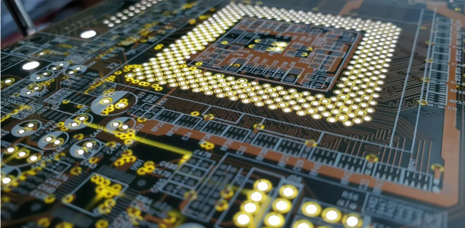
Table of Conent
Table of Conent
PCBs (Printed Circuit Boards) are an essential element in electronic design and manufacturing, serving as the backbone for all devices from calculators to supercomputers. Carrying various electronic components together, Printed Circuit Boards enable signal flow for their respective functions while protecting components against physical wear and tear.
As soon as you start your project, one of the primary decisions to be made is selecting between a Standard PCB and a Custom PCB. Your choice will have an immediate effect on performance, cost, development cycle and ultimate success of your endeavor. Understanding their fundamental differences will allow for the wisest and most economical technical decision. In this article we delve deeper into their definitions, characteristics and scenarios as a selection guide.
1. What is a Standard PCB?
A standard PCB, also known as a general-purpose PCB or perfboard/protoboard, refers to those circuit boards with a predefined, fixed layout. They are not designed for any specific application but instead provide a universal, flexible platform for engineers, hobbyists, and students to quickly build prototypes or conduct circuit experiments without going through a lengthy and expensive custom manufacturing process.
1.1 Main Types
- Breadboard:Completely solderless, used for the earliest stage of concept validation. Circuits are built temporarily by inserting wires and components, making modifications extremely easy. However, reliability is poor, making it unsuitable for permanent applications.
- Perfboard/Stripboard:The board features a regular array of pads with metallized through-holes. Users need to solder components themselves and use wires (typically fly wires or copper jumpers) to manually connect nodes according to the circuit diagram. This is an important step in transitioning from a breadboard to a more stable prototype.
- Universal Development/Evaluation Boards:Such as Arduino Uno, Raspberry Pi, ESP32 development boards, etc. These boards are usually built around a specific microcontroller or processor and have common interfaces (like USB, GPIO, Ethernet port) pre-connected. Users primarily program and connect peripheral devices to them rather than building the core circuit from scratch.
1.2 Core Characteristics
- Off-the-Shelf:Can be purchased directly from electronic component retailers, no need to wait for manufacturing.
- Extremely Low Cost:Single-board price is very cheap, suitable for experiments on a limited budget.
- High Flexibility:The same board can implement countless circuit functions through different wiring configurations.
- Fast Development Speed:Ideas can be implemented in hardware immediately, making it ideal for iteration and debugging.
- Obvious Limitations:The layout is not optimized, which can lead to high noise, poor signal integrity, and bulky size. Manual soldering and wiring are prone to errors, and large-scale repetitive production is completely impractical.
2. What is a Custom PCB?
A custom PCB is a circuit board specifically designed from the ground up according to the unique needs and functional requirements of a particular electronic product. Designers use Electronic Design Automation (EDA) software (such as Altium Designer, KiCad, Eagle, etc.) to precisely plan every detail of the board.
2.1 The design process
- Schematic Design:Drawing the logical connection diagram of the circuit.
- PCB Layout:Planning the board’s actual shape, size, component placement, and routing paths in the software.
- Rule Setting:Defining manufacturing parameters like trace width, clearance, layer stack-up structure, etc.
- Output Gerber Files:Generating a set of standard files containing precise image data for each layer (copper layers, silkscreen, solder mask, etc.), used by the PCB manufacturer for production.
2.2 Core Characteristics
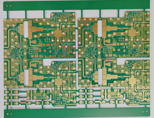
- Tailor-Made:Shape, size, number of layers, material, hole positions, and interface layout fully conform to the final product’s form and functional requirements.
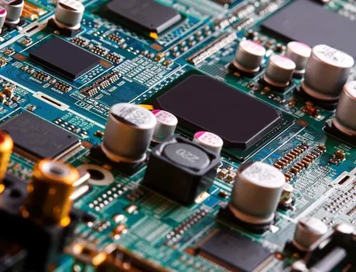
- Performance Optimization:Allows for fine-tuning of high-speed signals, impedance control, power distribution, thermal management, and Electromagnetic Compatibility (EMC), ensuring optimal electrical performance and reliability.
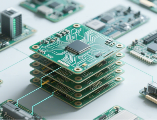
- High Integration and Miniaturization:Compact component layout and efficient routing minimize product volume to the greatest extent.
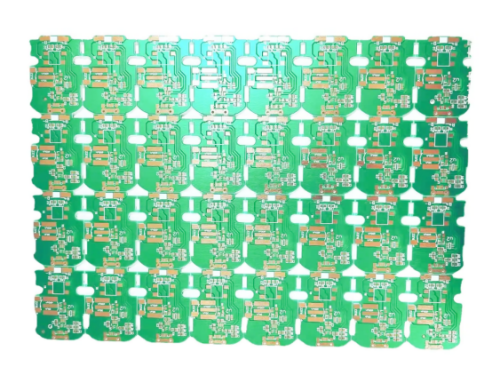
- Consistency and Reproducibility:Once the design is finalized, every board produced is completely identical, making it ideal for mass production.
- High Initial Investment:Requires investment of time for design and money for prototyping, but the unit cost decreases significantly in volume.
3. Key Differences between Custom PCBs and Standard PCBs
The following table compares custom PCBs and standard PCBs across several dimensions to help illustrate their respective distinctions:
| Characteristic Dimension | Standard PCB | Custom PCB |
| Design | Universal, fixed layout | Designed specifically for the application |
| Cost | Very low single-unit purchase cost | High initial design/prototyping cost, low bulk unit cost |
| Development Time | Almost zero, off-the-shelf | Long (design, prototyping, testing, modification) |
| Performance | Average, susceptible to noise and interference | High, optimized for signal integrity, EMC, etc. |
| Size & Shape | Fixed, usually rectangular | Arbitrary, can perfectly fit the product enclosure |
| Complexity | Low to medium, wiring done manually by user | Can achieve very high complexity (multi-layer stacks, HDI) |
| Consistency | Low (depends on user’s manual skill) | High (automated production, perfectly consistent) |
| Scalability | Almost impossible for mass production | Perfectly suited for small to large-scale production |
| Applicable Stage | Concept validation, learning, experimentation | Prototype validation, testing, mass production |
3.1 When to Use a Standard PCB
Standard PCBs are excellent tools in specific scenarios. Using them wisely can save significant time and resources.
- Education and Learning:For electronics engineering students and beginners, standard PCBs are an ideal platform for understanding circuit principles, practicing soldering, and debugging skills. They provide immediate practical feedback.Concept Validation and Prototype Iteration: When you have a preliminary idea and need to quickly verify whether a core function or circuit module is feasible, building the circuit on a breadboard or perfboard is the fastest and most economical way. It allows for frequent modifications and tests without paying prototyping fees and waiting days for each change.
- DIY Hobby Projects:If you are only making one or two personal projects for your own use (like a custom keyboard, a small decorative light) and have no strict requirements on size and appearance, using a perfboard for manual soldering is a completely viable solution.
- Extremely Low Volume Needs:When you only need to make 1-5 final products, the cost and time of custom PCB prototyping might outweigh the benefits, making manual fabrication a more reasonable choice.
In conclusion, if speed, versatility, and really low starting cost are your top priorities, standard PCBs are your best option.
3.2 When to Choose a Custom PCB
Custom PCBs become indispensable when your project moves beyond the initial experimental phase towards a more serious and professional direction.
- Product Enters Final Prototype and Testing Stage:Once the circuit functionality is verified on a perfboard, the next step is to create a prototype closer to the final product. Custom PCBs can expose issues like high-frequency effects and EMC that only appear with optimized layout and routing, enabling true product-level testing.
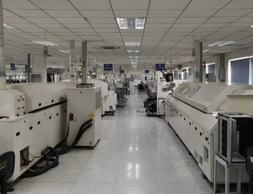
- Mass Production:This is the primary value proposition of custom PCBs. No company would manually solder thousands of perfboards to produce a product. The automated manufacturing process of custom PCBs ensures high efficiency, low cost, and extremely high consistency.
- Stringent Performance Requirements:If your design involves high-speed digital signals (e.g., HDMI, DDR memory), high-frequency RF circuits (e.g., Wi-Fi, Bluetooth modules), sensitive analog signals (e.g., audio amplification, sensor acquisition), or high-current power driving, you must use a custom PCB. Only through careful stack-up design, impedance control, grounding, and shielding planning can signal integrity and system stability be guaranteed.
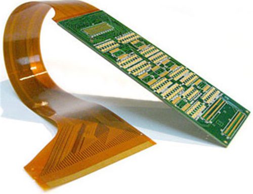
- Space-Constrained Applications:All consumer electronics (phones, smartwatches, TWS earbuds) intensely pursue miniaturization and lightweight design. Only custom PCBs can perfectly fit circuits into tight spaces through High-Density Interconnect (HDI), multi-layer board design, and the use of miniature components.
- High Requirements for Reliability and Durability:Products in fields like industrial equipment, automotive electronics, and medical devices must operate stably for years in harsh environments. Custom PCBs use high-quality substrates (e.g., FR-4, high-frequency laminates) and are produced under strict process standards, offering far greater reliability than hand-soldered perfboards.
- Brand and Aesthetics:Custom PCBs can have exquisite silkscreen layers (logos, component identifiers) and chosen solder mask colors (like the black commonly used in Apple products), enhancing the product’s overall professional feel and brand value.
In conclusion, if you want performance, dependability, manufacturability, miniaturization, and professionalism, you can only choose custom PCBs.
4. Why Custom PCBs Are Worth the Investment
Although initial design and prototyping costs are required, custom PCBs are an investment with a very high return in the long run.
- Reduces Overall Cost
In mass production, the unit price of custom PCBs can become very low. Automated production also saves significant manual soldering costs and time. While manual production seems to save on prototyping fees, its potential debugging, troubleshooting, and rework costs grow exponentially at scale.
- Enhances Product Value
A well-optimized PCB means better performance, smaller size, and higher reliability, which directly translates into stronger product competitiveness and higher market value.
- Avoids Future Problems
Solving potential signal and EMC issues during the design phase is far more cost-effective than dealing with product recalls or reputational damage after launch. The custom PCB design process itself is a form of risk control.
- Protects Intellectual Property
The design files for a custom PCB are your unique intellectual property. Products based on universal development boards are easily mimicked by competitors. A well-designed custom PCB is an important part of the technical barrier.
5. FAQ: Custom PCB vs. Standard PCB
1) What is the difference between a custom PCB and a standard PCB?
The most fundamental difference lies in specificity versus generality. A custom PCB is like a custom-made competition suit for an athlete, perfectly fitting the body and pursuing optimal performance; while a standard PCB is like a one-size-fits-all T-shirt that anyone can wear, but it may not fit perfectly. The former is optimized for a specific application, the latter provides a universal platform for users to build upon.
2) Are custom PCBs more expensive than standard PCBs?
This question needs to be viewed in stages. Single Acquisition Cost: Yes, the cost of custom PCB prototyping (e.g., 5 pieces), ranging from tens to hundreds of RMB, is much higher than buying a perfboard (a few to tens of RMB). Mass Production Cost: No, when the volume rises to hundreds or thousands of units, the unit price of custom PCBs becomes very low (possibly just a few RMB per piece), while the labor cost of manually soldering perfboards becomes unbearable. Therefore, custom PCBs have high initial costs but low marginal costs; standard PCBs have low initial costs but extremely high marginal (labor) costs.
3) When should I use a custom PCB?
You should use a custom PCB when your project meets any of the following conditions:
- Mass production is required.
- The circuit has high performance requirements (high-speed, high-frequency, high-precision).
- The product space is compact and requires miniaturization.
- There are professional requirements for product reliability and consistency.
- The project has completed preliminary concept validation using standard PCBs and needs to create formal prototypes.
4) Are standard PCBs suitable for beginners or DIY projects?
Extremely suitable. Standard PCBs are the cornerstone for beginners entering electronics. They are low-cost, provide immediate feedback, are easy to modify, and help newcomers quickly understand hardware knowledge and develop hands-on skills. They are also a perfect solution for DIY projects not pursuing commercialization and high performance.
5) Which is better, custom PCB or standard PCB?
There is no absolute “better,” only “more suitable.” They are tools for different stages and different goals.
- Standard PCBs are tools for exploration, learning, and rapid iteration.
- Custom PCBs are components for building the final product.
A successful product development process is often: Validate the core idea using standard PCBs (breadboard/perfboard) -> Create custom PCBs for engineering prototype testing and optimization -> Use the final custom PCB design for mass production.
6. Summary
Y&T Technology: Your Trustworthy Partner for Custom and Standard PCBs
To select PCBs successfully for any project, the key factor is understanding the current stage and ultimate goals. Whether your aim is capturing creative inspiration with perfboard soldering by hand or developing market-leading products using precisely manufactured custom PCBs, both are invaluable components of the innovation journey. Additionally, selecting a trustworthy manufacturing partner is essential when deciding to move forward with custom PCBs.
Latest Blog

Contact Info
Phone: +86-755-82882936
Email: [email protected]
WhatsApp: +86-13570802455
Wechat: +86-13570802455
Address: 2nd floor,D Bldg.,Electric Link Technology Bldg.,Gongming,Guangming New Dist.,518106 Shenzhen, China