PCB Panelization: Boost Efficiency & Cut Costs
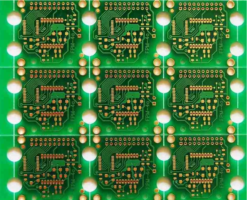
Table of Conent
Table of Conent
In the fast-paced world of electronics, efficiency and cost-effectiveness are paramount. Printed Circuit Boards (PCBs) are the foundation of virtually all electronic devices, and their manufacturing process is a complex dance of precision and speed. One crucial technique that significantly streamlines this process is PCB panelization. This method is the unsung hero behind mass-produced electronics, transforming individual board fabrication into a highly efficient, assembly-line operation.
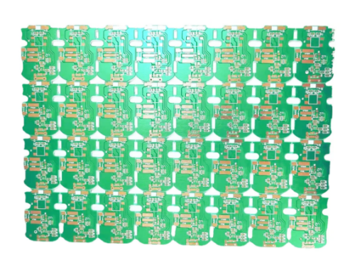
PCB panelization, often referred to as PCB array or PCB nesting, involves arranging multiple individual PCBs onto a larger, single panel. This panel is then processed as a single unit throughout various stages of fabrication and assembly, rather than handling each board separately. The result? A dramatic reduction in manufacturing time, material waste, and overall production costs. Whether you’re a seasoned PCB designer or a manufacturer looking to optimize your workflow, understanding the nuances of panelization is key to unlocking greater productivity and profitability.
1. What is PCB Panelization?
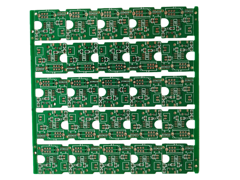
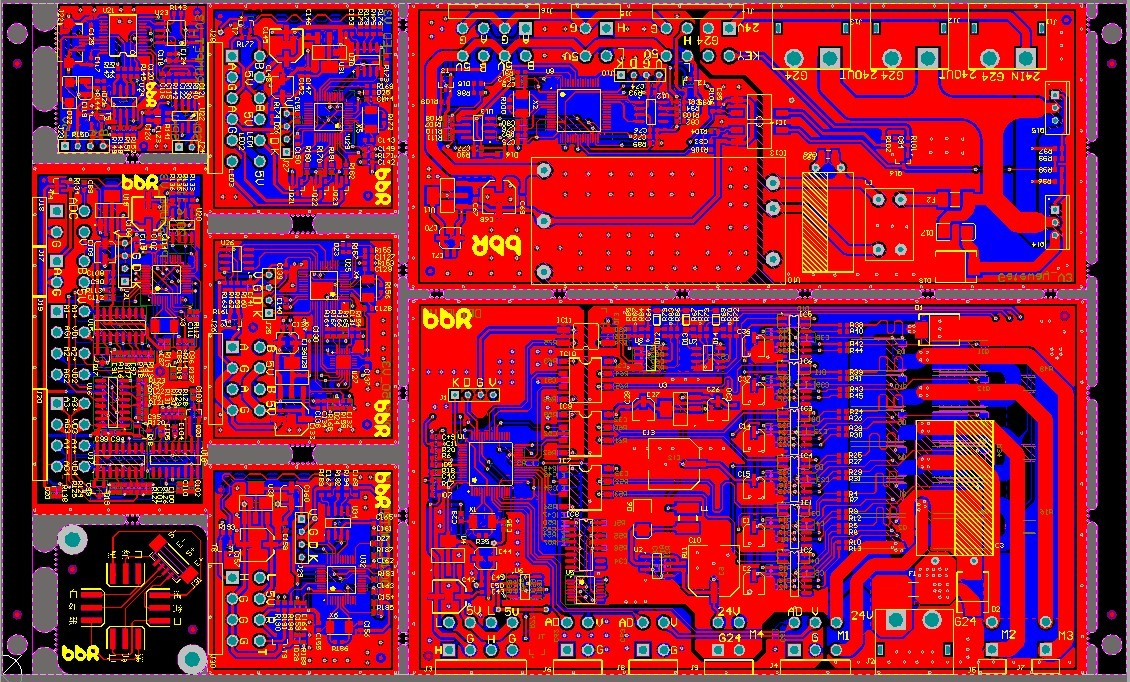
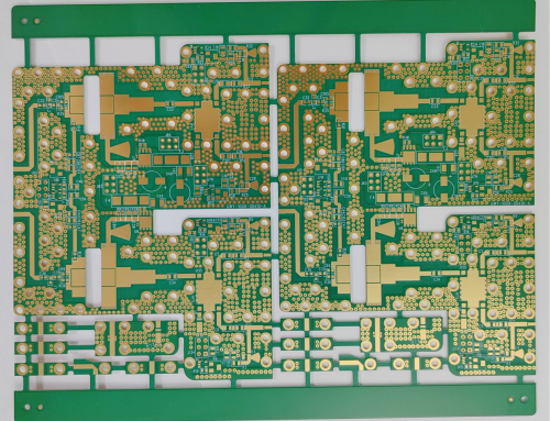
PCB panelization is a manufacturing practice where several individual printed circuit boards are grouped together onto a larger substrate, known as a panel or array, for simultaneous production. Instead of manufacturing and assembling each board independently, multiple identical or even different board designs are fabricated as a single unit. After all manufacturing and assembly processes are complete, these individual PCBs are then separated from the panel along pre-defined lines.
This method is widely adopted in high-volume PCB manufacturing due to its ability to drastically improve efficiency. By treating an array of boards as one, factories can maximize the use of their equipment, such as pick-and-place machines for automated assembly, reflow ovens, and soldering systems . This centralized processing minimizes the number of times equipment needs to be set up or reconfigured, thereby saving valuable time and labor. The ultimate goal of panel design is to optimize the manufacturing process from start to finish, ensuring a smooth transition through each stage of production.
2. Why Panelize? Unpacking the Benefits
The importance of PCB panelization cannot be overstated for modern PCB manufacturing and PCB assembly. It offers a multitude of advantages that directly impact a project’s bottom line and timeline. Here are the primary benefits:
- Enhanced Efficiency and Throughput:By processing multiple boards concurrently, manufacturers can achieve higher production volumes in less time. This parallel processing significantly reduces cycle times, making it ideal for large-scale production runs and improving the overall efficiency of the assembly line.
- Significant Cost Reduction:Cost reduction is perhaps the most compelling benefit. Panelization minimizes setup times for machinery, reduces material handling costs, and optimizes the use of raw materials by tightly nesting designs. This economy of scale translates to lower per-board production costs, making projects more competitive.
- Improved Handling in Automated Assembly:Individual small PCBs can be difficult to handle with automated assembly equipment. A larger, rigid panel provides a stable substrate that is easier to transport, load into machines, and manage throughout the assembly process. This reduces the risk of damage and ensures consistent placement.
- Reduced Material Waste:Intelligent panel design allows for better utilization of raw PCB laminate material. By arranging multiple boards, designers can minimize the unused space on a panel, leading to less scrap material and greater sustainability.
- Consistent Quality and Reliability:Processing boards in a panel ensures that each unit undergoes the same manufacturing conditions simultaneously. This consistency helps in maintaining uniform quality across all boards, reducing variations that might occur if each board were processed individually.
- Streamlined Testing:A panel can often be tested as a whole or in sections before individual boards are broken apart. This can simplify and speed up functional testing, further contributing to efficiency.
Ultimately, panelization is a strategic choice that boosts manufacturing capabilities, cuts expenses, and ensures the reliability of the final electronic product.
3. Key Techniques for PCB Panelization
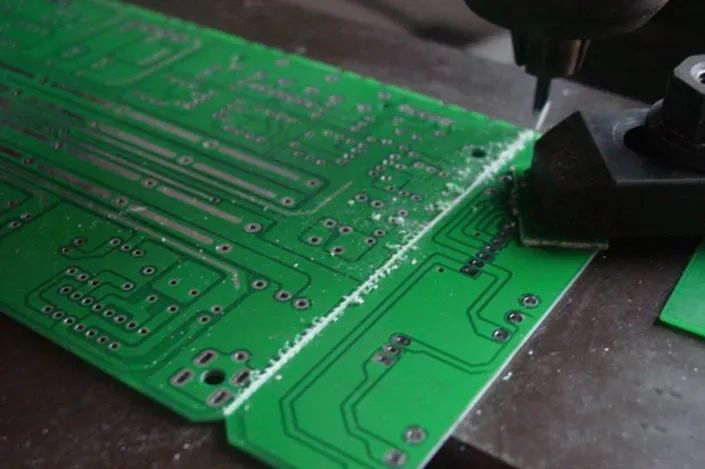
The method chosen for separating individual PCBs from the panel is a critical design tip that influences the entire panel design and subsequent PCB assembly. The two most common and effective techniques are V -scoring and tab routing, each with distinct advantages and applications.
V-Scoring (V-Groove)
V-scoring, also known as V-grooving, involves cutting a V-shaped groove into the top and bottom surfaces of the PCB panel. These grooves are made along the lines where the individual boards will eventually be separated. The remaining material in the middle acts as a weak point, allowing the boards to be ” snapped” apart manually or with a specialized depaneling machine after PCB assembly.
1) How it works: A rotary cutter makes a precise V-cut, typically about one-third of the board thickness, on both sides of the panel. The remaining material in the center ensures structural integrity during manufacturing and assembly.
2) Advantages:
- Cost-effective for high-volume production.
- Faster separation process compared to routing.
- Produces clean edges, provided the snap-off is executed correctly.
- Requires minimal space between boards, optimizing material usage.
3) Limitations:
- Only suitable for boards with straight-line separation. Complex shapes or curves cannot be V-scored.
- Components cannot be placed too close to the V-score lines (typically within 0 .5mm) to prevent damage during depaneling.
- Can generate some stress on components during separation.
Tab Routing (Breakaway Tabs)

Tab routing, or using breakaway tabs, involves routing the outline of each individual PCB on the panel, but leaving small, unrouted sections (tabs) that connect the board to the panel frame or to adjacent boards. These tabs are typically perforated with “mouse bites” (small holes) to weaken them, making separation easier.
1) How it works: A router cuts the board outlines, leaving 2-5 small tabs (often 0 .5mm to 2mm wide) along the perimeter of each board. These tabs are designed to be easily broken post-assembly.
2) Advantages:
- Allows for boards with complex shapes, curves, and internal cutouts.
- Components can be placed closer to the board edge compared to V-scoring.
- Less stress on components during separation, especially with well-designed mouse bites.
- Offers greater design flexibility.
3) Limitations:
- Generally slower and more expensive than V-scoring due to routing time.
- Requires more spacing between boards for the router bit.
- Edges may not be as perfectly smooth as V-scored boards, often requiring light sanding or filing after breaking, especially if the tabs are large or poorly designed.
- The “mouse bites” can sometimes leave small burrs.
Comparison of Panelization Techniques
Here’s a quick overview comparing the two methods:
| Feature | V- Scoring | Tab Routing (Breakaway Tabs) |
| Separation Line | Straight lines only | Complex shapes, curves, internal cutouts |
| Cost Efficiency | Generally lower for high volume | Generally higher due to routing time |
| Component Proximity to Edge | Needs clearance (~0.5mm) | Can be closer to edge |
| Edge Quality | Clean snap -off, smooth edge | May have small burrs from tabs |
| Panel Space | Minimal space between boards | Requires wider gaps for router bit |
4. Crucial Design Considerations for Effective Panelization
Successful PCB panelization isn’t just about choosing a separation method; it requires careful attention to several design tips and best practices. These considerations ensure optimal PCB manufacturing and PCB assembly processes, leading to high-quality, cost-effective outcomes.
Component Placement and Keep-Out Zones
One of the most critical aspects is the placement of components, especially for boards that will be separated using V-scoring or breakaway tabs.
- For V-scoring, ensure that no components, traces, or pads are placed directly over the V-groove lines. A minimum keep-out distance (typically 0.5mm to 1mm) from the score line is essential to prevent damage during depaneling.
- With tab routing, components can be placed closer to the board edge, but it’s still advisable to maintain a small clearance from the tabs themselves, especially if they contain “mouse bites,” which can cause localized stress. Avoid placing heavy components near the breakaway tabs.
Failing to observe these zones can lead to cracked components, lifted pads, or compromised solder joints when the boards are separated.
Fiducials and Tooling Holes
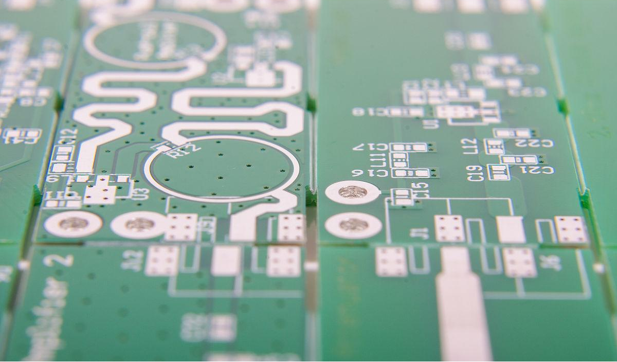
For automated assembly, accurate alignment is paramount. Fiducials are copper pads or shapes placed on the panel design and individual PCBs that act as reference points for vision systems on pick-and-place machines.
- Global Fiducials:Placed on the panel’s edge rails , these align the entire panel with the assembly equipment.
- Local Fiducials:Placed on individual PCBs (often in pairs), these help the machine precisely align specific components, especially fine-pitch devices.
Tooling holes (or registration holes) are non-plated through-holes strategically placed on the edge rails of the panel. These holes allow the panel to be accurately pinned and secured onto assembly jigs, conveyors, or testing fixtures, ensuring consistent positioning throughout the process.
Edge Rails and Clearances
Edge rails, also known as “breakaway rails” or “tooling strips,” are strips of material added to the perimeter of the PCB panel. They serve multiple purposes:
- Provide structural integrity to the panel during handling and assembly.
- Offer space for global fiducials, tooling holes, and barcodes for traceability .
- Facilitate clamping by automated assembly equipment without interfering with the active circuitry.
Adequate spacing between individual PCBs on the panel and between the PCBs and the edge rails is crucial. This clearance is necessary for the router bit during tab routing or to prevent components from encroaching on the V-score lines. Typical spacing ranges from 1.5mm to 3mm, depending on the chosen separation method and manufacturer capabilities.
Panel Size and Layout Optimization
Choosing an appropriate standard panel size is important, as manufacturers often work with specific dimensions to maximize equipment utilization. The panel design should optimize the number of boards per panel without compromising manufacturing tolerances or component placement. Consider factors like board orientation to facilitate efficient automated assembly and solder paste printing, especially for double-sided boards. Rotating some boards 90 or 180 degrees can sometimes improve cost reduction by allowing more boards to fit within a given panel area.
5. Overcoming Panelization Challenges
While PCB panelization offers significant benefits, it’s not without its complexities . Awareness of these challenges allows designers and manufacturers to proactively implement solutions, ensuring a smoother PCB manufacturing and PCB assembly process.
- Component Placement Constraints:As discussed, components near panel edges or separation lines can be vulnerable to stress or damage during depaneling. Careful design tips regarding keep-out zones are essential to mitigate this.
- Thermal Management:If the individual PCBs generate significant heat, arranging them closely on a panel can exacerbate thermal issues during reflow soldering. The combined thermal mass needs to be considered to ensure proper solder joint formation without overheating components.
- Manufacturing Tolerances:Even with precision equipment, there are inherent manufacturing tolerances . These can affect the accuracy of V-scoring or tab routing, potentially leading to uneven breaks or slight shifts in board dimensions after separation.
- Assembly and Testing Considerations:While panelization aids automated assembly, testing requirements for panels can sometimes be more complex than for individual boards. Developing panel-level test fixtures requires careful planning.
- Cost vs. Complexity:For very small production runs or highly unique board shapes, the upfront cost and design effort of panelization might outweigh the benefits. Balancing cost reduction with the complexity of panel design is key.
6. Tools for PCB Panelization
Modern Electronic Design Automation (EDA ) software plays a pivotal role in optimizing PCB panelization. Tools like Altium Designer, Eagle, KiCad, and Cadence Allegro (mentioned in one source’s context) offer functionalities that assist designers in creating efficient panel layouts. These software packages can help with:
- Arranging multiple instances of a board design or different designs onto a panel.
- Defining V-scoring lines or tab routing paths with “mouse bites.”
- Adding fiducials, tooling holes, and edge rails.
- Performing design rule checks (DRC) to ensure clearances and prevent issues with component placement near separation lines.
- Generating the necessary output files ( Gerber files, drill files) that the PCB manufacturing facility uses to produce the panel.
Utilizing these specialized tools is crucial for ensuring the quality, reliability, and manufacturability of the final product while maximizing efficiency and cost reduction.
7. PCB Panelization FAQs
8. Summary
PCB panelization is an indispensable technique in modern PCB manufacturing, enabling manufacturers to produce electronic circuits with unparalleled efficiency and significant cost reduction. By grouping multiple PCBs onto a single panel, the entire fabrication and automated assembly process is streamlined, minimizing material waste and optimizing equipment utilization. Key panelization methods like V-scoring and tab routing (with breakaway tabs) offer distinct advantages, catering to different board geometries and production needs. Successful implementation hinges on careful design tips, including strategic component placement, the incorporation of fiducials and tooling holes for alignment, and well-designed edge rails. Despite challenges such as thermal considerations and manufacturing tolerances, leveraging specialized software tools allows for the creation of robust panel design solutions. For any designer or manufacturer aiming to scale production, boost efficiency, and ensure the quality of their electronic products, mastering PCB panelization is not just an option—it’s a necessity.
Key Takeaways
- Efficiency is Key:PCB panelization dramatically boosts efficiency in PCB manufacturing by processing multiple boards simultaneously.
- Cost Savings are Real:It leads to substantial cost reduction by optimizing material usage, reducing setup times, and improving automated assembly throughput.
- Choose Wisely:V-scoring is best for straight-edged boards, while tab routing with breakaway tabs offers flexibility for complex shapes .
- Design for Success:Proper component placement, fiducials, tooling holes, and edge rails are critical for a flawless panel design.
- Leverage Technology: Utilize EDA software to effectively plan and execute your PCB panelization strategy.
Latest Blog
Contact Info
Phone: +86-755-82882936
Email: [email protected]
WhatsApp: +86-13570802455
Wechat: +86-13570802455
Address: 2nd floor,D Bldg.,Electric Link Technology Bldg.,Gongming,Guangming New Dist.,518106 Shenzhen, China