Ultra-Thin PCB: The Future of Electronics Design
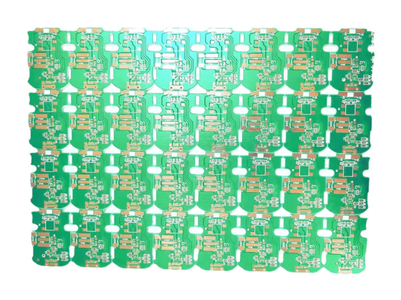
Table of Conent
Table of Conent
In an era defined by compact electronics and ever-shrinking devices, the demand for smaller, lighter, and more powerful components has never been higher. From the smartphone in your pocket to life-saving medical implants, the drive towards miniaturization is relentless. At the heart of this revolution lies the ultra-thin PCB(Printed Circuit Board)–a groundbreaking technology that’s reshaping what’s possible in modern electronics design. These cutting-edge circuit boards are not just thinner; they are enabling new functionalities, enhancing performance, and opening doors to innovative product designs previously unimaginable.
This comprehensive guide aims to transform you into an ultra-thin PCB expert, exploring everything from their fundamental definition and the specific materials that make them possible, to their intricate manufacturing challenges and the vast array of applications where they shine. Whether you’re an engineer, a product designer, a purchaser, or simply curious about this pivotal technology, prepare to dive deep into the world of ultra-thin PCBs and discover how they are quietly powering the next generation of advanced electronics.
1. What Exactly Are Ultra-Thin PCBs?
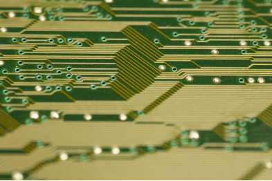
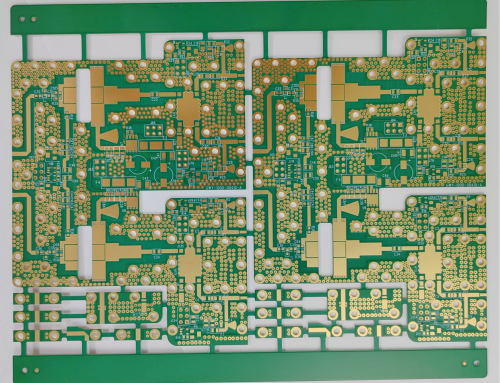
An ultra-thin PCB is a specialized type of printed circuit board characterized by its remarkably reduced thickness compared to standard PCBs. While traditional rigid PCBs often measure around 1.6mm (0.063 inches), ultra-thin PCBs can range from as little as 0.1mm to 0.4mm (0.004 to 0.016 inches). This significant reduction in thickness is achieved through advanced material selection and precise manufacturing processes.
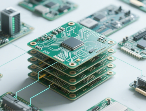
These boards are not merely scaled-down versions; they often incorporate flexible or semi-flexible substrates, making them highly adaptable to complex geometries and tight spaces. The core concept behind their development is to maximize functionality within minimal volume and weight, without compromising performance or reliability. They are crucial for creating high density interconnects (HDIs) in compact devices where every millimeter counts.
2. The Unrivaled Benefits of Ultra-Thin PCBs
The advantages of incorporating ultra-thin PCBs into electronic designs are numerous, directly addressing many of the challenges faced by modern product developers:
- Space Savings :This is perhaps the most obvious benefit. By significantly reducing the Z-axis dimension, ultra-thin PCBs free up valuable internal space in electronic This allows for smaller overall device footprints or the integration of more components and features within existing form factors.
- Weight Reduction:Less material means less weight. For portable devices, wearables, and aerospace applications, every gram matters. Ultra-thin PCBs contribute significantly to creating lighter products, enhancing user comfort and operational efficiency.
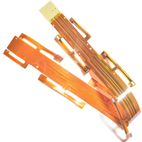
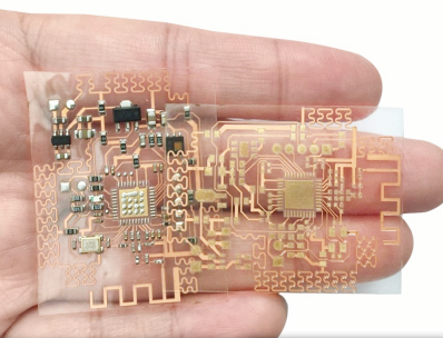
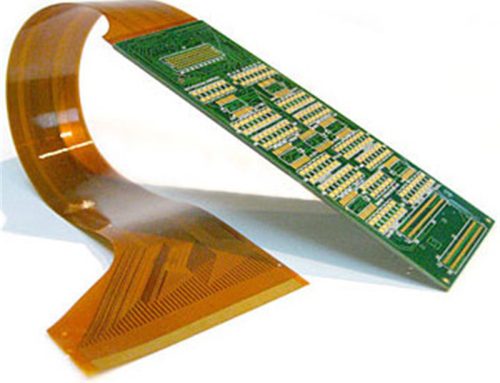
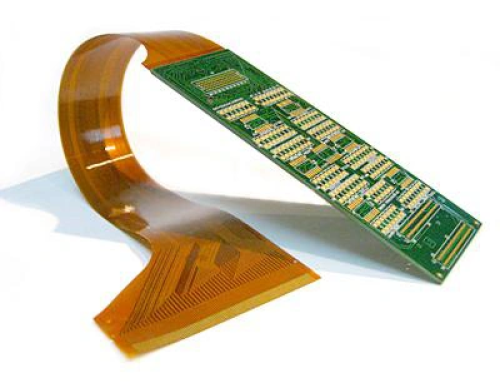
- Enhanced Flexibility:Many ultra-thin PCBs are inherently flexible (often referred to as ultra-thin flex PCBs). This flexibility allows them to bend, fold, and twist, conforming to irregular shapes and tight contours. This capability is vital for innovative designs like foldable smartphones, wearable sensors, and medical devices that must adapt to the human body.
- Improved Heat Dissipation:While counter-intuitive, thinner substrates can sometimes offer better thermal paths, especially when combined with appropriate materials and thermal management strategies. The reduced distance for heat to travel can aid in dissipation.
- Higher Signal Integrity:In certain high-frequency applications, a thinner dielectric layer (the insulating material between copper layers) can lead to better impedance control and reduced signal loss, contributing to superior electrical performance.
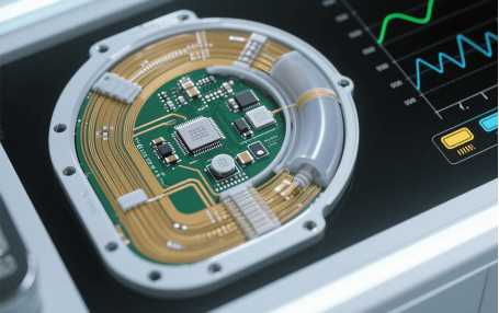
- Miniaturization and Integration:Ultra-thin PCBs are key enablers for miniaturization, allowing the integration of complex circuits into extremely small packages. This drives innovation in areas like micro-sensors, implantable devices, and high-density computing modules.
3. Key Materials for Ultra-Thin PCB Fabrication
Choosing the right substrate material is paramount in the design and manufacture of ultra-thin PCBs. The material selection impacts not only the mechanical properties like flexibility and durability but also critical electrical characteristics such as dielectric constant for thin PCB designs and thermal resistance. Here are the most common types:
FR4 Thin PCB
FR4 (Flame Retardant 4) is the most widely used material for rigid PCBs due to its excellent balance of electrical, mechanical, and thermal properties, along with its cost-effectiveness. When used for ultra-thin PCBs, special, thinner prepregs and laminates are employed. An FR4 thin PCB is typically used in standard ultra-thin applications where some rigidity is still desired, but overall thickness needs to be minimized. It offers good dielectric strength and is suitable for many commercial and consumer electronics.
Polyimide Thin PCB
Polyimide is the workhorse for flexible and high-temperature ultra-thin PCBs. Its outstanding mechanical flexibility, excellent thermal stability (withstanding high temperatures without degradation), and superior electrical properties make it ideal for ultra-thin flexible PCB applications. An polyimide thin PCB is often found in devices requiring continuous bending or operation in harsh environments, such as medical implants, wearable technology, and automotive sensors. Its low dielectric constant also makes it suitable for high-frequency designs.
BT Material Thin PCB
BT (Bismaleimide Triazine) material is a high-performance resin system known for its superior thermal reliability, low dielectric constant, and low dissipation factor. These characteristics make a BT material thin PCB an excellent choice for advanced, high-frequency, and high-speed applications. It offers better performance at higher temperatures and frequencies compared to standard FR4, making it suitable for telecommunications equipment, servers, and high-performance computing.
Here’s a comparative overview of these common ultra-thin PCB materials:
| Material Type | Key Characteristics | Typical Applications | Pros | Cons |
| FR4 (Thin) | Good balance of properties, cost-effective, rigid | Consumer electronics, standard devices, general ultra-thin applications | Affordable, widely available, good electrical properties | Limited flexibility, lower thermal performance than advanced materials |
| Polyimide (Thin) | Excellent flexibility, high thermal resistance, low dielectric constant | Flexible PCBs, wearables, medical implants, high-temperature environments | Highly flexible, durable, excellent thermal stability | Higher cost, requires specialized manufacturing processes |
| BT Material (Thin) | High thermal reliability, low dielectric constant, low dissipation factor | High-frequency applications, advanced computing, telecommunications | Superior high-frequency performance, excellent thermal reliability | Higher cost, less flexible than polyimide |
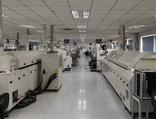
4. Manufacturing Ultra-Thin PCBs: Precision and Challenges
The production of ultra-thin PCBs demands extreme precision and specialized techniques, introducing several unique challenges compared to standard PCB manufacturing:
- Material Handling:Ultra-thin substrates, especially flexible ones, are delicate and prone to warping, tearing, or creasing. Specialized equipment and controlled environments are necessary for handling these materials throughout the fabrication process, from lamination to etching.
- Drilling and Plating:Creating precise microvias and through-holes in thin materials requires advanced drilling technologies like laser drilling. Subsequent plating processes must ensure uniform copper deposition without damaging the thin substrate or causing aspect ratio issues.
- Etching and Fine Lines:Achieving extremely fine trace widths and spaces is critical for high-density interconnects in ultra-thin PCBs. This requires highly controlled etching processes to prevent over-etching or under-etching, which could compromise signal integrity.
- Lamination:For multi-layer ultra-thin PCBs, precise alignment and void-free lamination are challenging. The thin layers can easily shift or entrap air, leading to defects. Vacuum lamination and specialized press cycles are often employed.
- Thermal Management:While thinness can aid heat dissipation, the high component density on compact designs can also lead to localized hot spots. Effective thermal management solutions, such as thermal vias or specialized heat sinks, must be integrated carefully.
- Quality Control:Inspection and testing of ultra-thin PCBs require high-resolution imaging and sophisticated electrical testing equipment to detect subtle defects that might not be visible or critical in thicker boards.
5. Diverse Applications: Where Ultra-Thin PCBs Thrive
Ultra-thin PCBs are essential enablers across a wide range of industries, driving innovation and making previously impossible designs a reality:
- Wearable Technology:Smartwatches, fitness trackers, smart glasses, and electronic textiles rely heavily on ultra-thin and flexible PCBs to conform to the body and maintain a lightweight, unobtrusive profile.
- Medical Devices:From implantable pacemakers and neurostimulators to miniature hearing aids and endoscopic cameras, ultra-thin PCBs enable the creation of tiny, high-performance medical electronics that can safely interact with the human body.
- Smartphones and Tablets:The constant push for thinner, lighter, and more powerful mobile devices necessitates ultra-thin PCBs to pack more features into shrinking form factors. This includes components like display drivers, camera modules, and internal antennas.
- Aerospace and Defense:Weight reduction and reliability are paramount in aerospace. Ultra-thin PCBs are used in avionics, satellite systems, and drone technology, where every gram saved contributes to fuel efficiency and performance.
- Automotive Electronics:As vehicles become more connected and autonomous, ultra-thin PCBs are finding their way into advanced driver-assistance systems (ADAS), infotainment systems, and flexible lighting solutions, contributing to compact electronics.
- High-Frequency Communication:For 5G modules, Wi-Fi 6/7, and other high-speed data transmission systems, ultra-thin PCBs with low dielectric constant materials are crucial for maintaining signal integrity and minimizing losses.
- Industrial Sensors:Miniature sensors for environmental monitoring, industrial automation, and IoT devices benefit from the small size and durability offered by ultra-thin PCB technology.
6. Future Trends in Ultra-Thin PCB Technology
The evolution of ultra-thin PCBs is far from over, with ongoing research and development promising even more exciting advancements:
- Further Miniaturization:The drive for even thinner boards and finer features will continue, pushing the boundaries of material science and manufacturing precision.
- Enhanced Functionality:Integration of more advanced functionalities directly onto the PCB, such as embedded components (passives and active ICs), will become more common, leading to even greater component density and smaller modules.
- Advanced Materials:Development of new substrate materials with improved thermal management, higher frequency performance, and greater environmental resilience will be key. This includes novel ceramic-based or polymer-composite materials.
- Increased Flexibility and Stretchability:Beyond simple flexibility, future ultra-thin PCBs may offer stretchable properties, making them ideal for highly dynamic wearable applications, e-textiles, and bio-integrated electronics.
- Sustainability:Research into more environmentally friendly manufacturing processes and recyclable or biodegradable ultra-thin PCB materials will gain traction, aligning with global sustainability goals.
- Hybrid Approaches:The combination of rigid and flexible ultra-thin sections (rigid-flex PCBs) will become more sophisticated, allowing for intricate 3D interconnect solutions that optimize space and performance.
7. Ultra-Thin PCB FAQs
8. Summary
Ultra-thin PCBs are more than just a slimmer version of traditional circuit boards; they are a cornerstone of modern electronics, essential for driving miniaturization, enhancing flexibility, and improving performance across a myriad of applications. From consumer electronics to critical medical and aerospace systems, their ability to deliver complex functionality in minimal space and weight is unparalleled. While their manufacturing presents significant challenges, ongoing advancements in materials and processes continue to push the boundaries of what these tiny titans can achieve, ensuring their pivotal role in the future of compact electronics and innovative design.
Key Takeaways
- Ultra-thin PCBs are crucial for miniaturization, reducing device size and weight by offering board thicknesses as low as 0.1mm.
- They provide significant benefits including space savings, weight reduction, enhanced flexibility, and improved signal integrity.
- Key materials for ultra-thin PCB materials include FR4 (for standard needs), polyimide (for flexibility and high temperatures), and BT material (for high-frequency/high-thermal performance).
- Manufacturing ultra-thin PCBs demands extreme precision, facing challenges in material handling, drilling, etching, and lamination.
- They are indispensable in diverse sectors such as wearables, medical implants, smartphones, aerospace, and high-frequency communication.
- Future trends point towards even greater miniaturization, advanced functional integration, and the development of sustainable, stretchable materials.
Latest Blog

Contact Info
Phone: +86-755-82882936
Email: [email protected]
WhatsApp: +86-13570802455
Wechat: +86-13570802455
Address: 2nd floor,D Bldg.,Electric Link Technology Bldg.,Gongming,Guangming New Dist.,518106 Shenzhen, China