
Flying Probe vs. Bed-of-Nails Testing: Compare Setup and Lifetime Costs
Table of Conent
Table of Conent
Flying probe and bed-of-nails testing can both check PCB assemblies for electrical manufacturing defects, but they create different cost and schedule profiles. Flying probe uses moving test heads and usually avoids a dedicated contact fixture, which reduces initial tooling and supports prototypes or changing designs. Bed-of-nails in-circuit testing uses a board-specific fixture with many spring probes contacting test points at once, which increases non-recurring setup but can provide much faster throughput for a stable, accessible, higher-volume design.
The correct choice is not simply “low volume versus high volume.” Compare required fault coverage, board access, program development, fixture design, cycle time, revision risk, maintenance, retest strategy, and expected lifetime quantity. Neither method replaces a defined functional test when product behavior must be verified under powered operating conditions.
What is the practical difference between the two methods?
A flying probe system moves a limited number of probes between accessible pads, vias, or test points under software control. It can be programmed from manufacturing and netlist data without a conventional full-contact fixture. A bed-of-nails system places many probes in a dedicated fixture so the tester can contact numerous nodes during the same cycle. This physical difference drives the tradeoff between flexibility and recurring test speed.
| Decision factor | Flying probe | Bed-of-nails ICT |
|---|---|---|
| Dedicated fixture | Usually not required for electrical contact | Board-specific probe fixture required |
| Initial engineering | Program, data preparation, debug, and access review | Fixture design/build plus program and debug |
| Cycle time | Probes move sequentially; generally slower | Many nodes contact together; generally faster |
| Design changes | Software changes may accommodate accessible revisions | Fixture modification or replacement may be needed |
| Typical fit | Prototype, NPI, low volume, changing designs | Stable repeat production with adequate access |
These are general tendencies, not guaranteed capabilities. Equipment, board complexity, access, measurements, automation, panel format, and coverage targets can change the result. Ask the test provider to estimate the actual program, fixture, cycle, and coverage for the released board.
Which costs belong in a complete comparison?
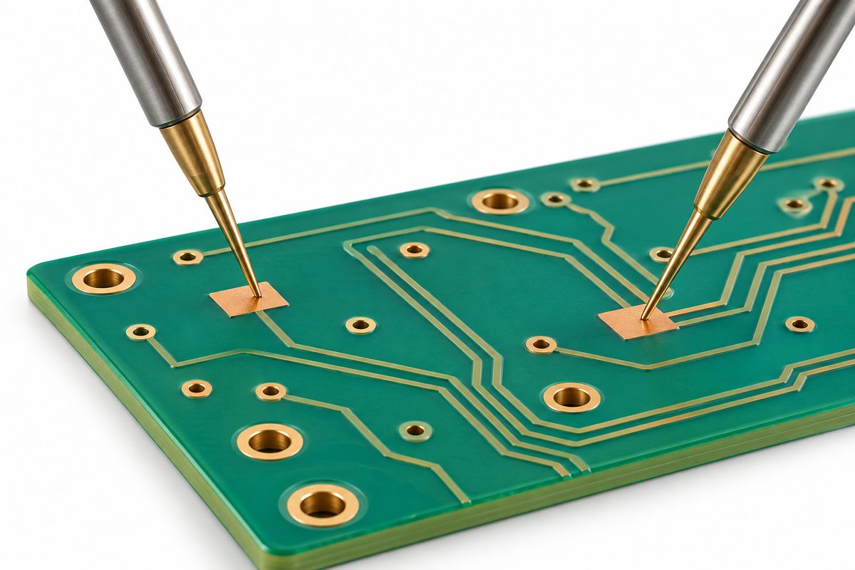
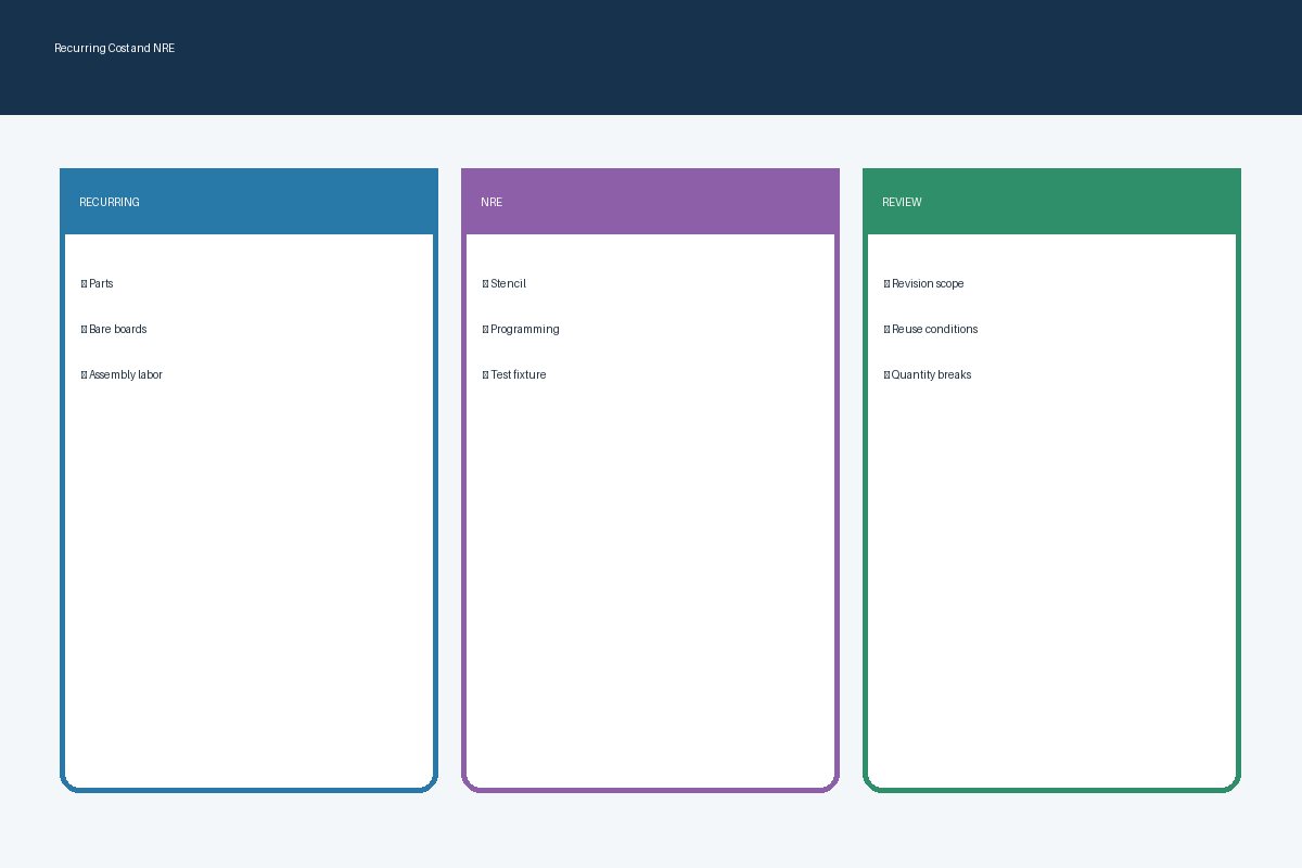
Total test cost includes more than the quoted fixture line item. Separate non-recurring engineering from recurring cost, then add likely revision and support costs over the planned product life. A low initial price can be misleading if cycle time constrains production; a fast fixture can be poor value if the board changes before its tooling is recovered.
- Test-strategy and access review
- Data preparation and program development
- Fixture design, fabrication, validation, and storage
- Debug boards, golden samples, and engineering support
- Tester time and operator or automation time per unit
- Probe cleaning, replacement, calibration, and fixture maintenance
- Failure diagnosis, false-call review, and retest handling
- Board revisions, variants, panels, and product transfer
- Reports, traceability, and data retention
The PCBA quote breakdown explains why tooling and test development should be separated from recurring component and assembly charges. Requesting one blended unit price can hide which costs will repeat and which depend on lifetime volume.
How can you estimate the lifetime break-even point?
Use a project-specific cost model instead of a generic quantity threshold. Let the fixture-based option have a higher initial cost but a lower recurring test cost. The simple break-even quantity is the difference in initial cost divided by the difference in per-unit test cost, provided the same boards, coverage, yield, retest policy, and overhead are being compared.
For example, if a hypothetical bed-of-nails solution adds $8,000 of fixture and engineering cost but saves $4 per tested unit compared with flying probe, the simple break-even is 2,000 units. That example is not a market price. Real decisions also include fixture maintenance, spare fixtures, tester availability, revision probability, panel utilization, false calls, diagnostics, and the financial effect of slower throughput.
Model several production scenarios: prototype only, pilot plus one volume release, expected repeat orders, and a revision after validation. A design with uncertain demand may preserve cash and flexibility with flying probe even if a high-volume forecast favors a fixture. A stable product with sustained demand may justify fixture investment earlier when test time limits line output.
How does PCB test access affect both choices?
Neither method can measure every node without physical and electrical access. Probe size, exposed contact area, spacing, component clearance, board-edge clearance, solder mask, coating, support, and probe approach must match the selected equipment. A pad that exists in CAD can still be blocked by a connector, shield, adhesive, fixture support, or populated variant.
Bed-of-nails fixtures need repeatable board location and a stable contact field. Dense designs may require double-sided or clamshell arrangements, added support, or accepted coverage gaps. Flying probes offer more routing flexibility but still need a reachable surface and enough movement clearance. Extremely small, crowded, or sensitive nodes may be impractical or electrically unsuitable for either method.
Use the PCB test point design guide to review contact geometry, populated clearance, electrical loading, coordinate data, and revision control before layout freeze. If access is deferred until production, the “cheaper” test method may require redesign or manual workarounds.
What fault coverage can each method provide?
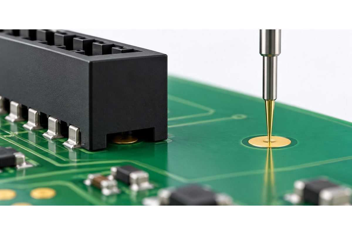
Coverage depends on the implemented program, not the method name. Possible checks include shorts, opens, resistance, capacitance, diode junctions, device orientation, component presence, powered measurements, programming, or boundary-scan integration. Actual capability depends on access, circuit topology, equipment resources, isolation techniques, limits, and customer requirements.
Do not report “100% tested” without defining the denominator. Distinguish component coverage, pin coverage, net coverage, structural defect coverage, and functional requirement coverage. Connected components can mask measurements. Parallel paths may prevent a simple value check. An accessible node may have no programmed test, while a functional test can exercise behavior without isolating the exact failed component.
Keysight describes bed-of-nails and flying probe as two in-circuit approaches, with dedicated-fixture speed versus fixtureless flexibility as a central distinction. SPEA likewise notes that flying probe programs can be generated from CAD data without a product-specific interface fixture. Vendor descriptions explain architecture; only a board-specific coverage review establishes what the planned test will detect.
When is flying probe the stronger choice?
Flying probe is often the stronger choice when designs change, quantities are limited, fixture lead time would delay learning, or several variants share only part of their access. It can support prototype and new-product-introduction feedback before committing to production tooling. Program changes may be easier than physical fixture changes when test points move but remain reachable.
It is not free of setup. The team still needs correct CAD or test data, net information, component attributes, board dimensions, panel data, access definitions, limits, and debug units. Cycle time can grow with node count and test complexity. Production planning should use the provider’s estimated time for the actual program, including load/unload, retries, reporting, and failure diagnosis.
Preparing an NPI build? Send Gerbers, BOM, pick-and-place data, netlist or agreed test data, assembly drawings, quantities, revisions, and coverage requirements through the engineering and quotation review. This allows fabrication, assembly, probe access, testing, and reporting to be scoped together.
When is bed-of-nails ICT the stronger choice?
Bed-of-nails ICT is often stronger when the design is stable, production volume is sustained, adequate test access exists, and cycle time matters. Parallel or near-simultaneous contact can reduce recurring test time, and the fixture can support repeatable production handling. It may also integrate specific powered or boundary-scan steps, depending on the system and program.
The fixture becomes a controlled production asset. Define fixture revision, board compatibility, alignment and support, wiring documentation, validation status, preventive maintenance, spare pins and interface parts, storage conditions, and transfer ownership. A correct fixture for revision A can produce false calls or physical interference on revision B.
Include expected lifetime quantity, lot cadence, panel format, variants, target cycle time, debug responsibilities, and fixture ownership when requesting a bed-of-nails test quotation. The quote should state what is included in fixture build, program development, validation, maintenance, and future revisions.
How should revisions and variants be handled?
Revision risk belongs in the economic model. Compare old and new test-point coordinates, populated clearances, nets, BOM variants, panelization, firmware, and test limits before reusing a program or fixture. A mechanical change near a probe can matter even when the schematic net is unchanged. A BOM variant can change expected measurements without moving copper.
Maintain a compatibility matrix linking board revision, BOM variant, panel revision, test program, fixture, firmware, and limit set. Require a documented review before release. Flying probe may reduce physical rework, but its program and expected values still need control. Bed-of-nails may support replaceable probe plates or modifications, but that possibility must be verified with the fixture supplier.
How do these tests fit with AOI, X-ray, and functional test?
Structural electrical testing complements rather than replaces other inspection. AOI evaluates visible placement and solder features. X-ray provides evidence for hidden joints. In-circuit methods can locate selected electrical defects and component issues. Functional test verifies defined product behavior under powered conditions. Boundary scan can improve access to supported digital interconnects.
The PCB assembly process guide places these methods within the complete manufacturing route. Build a detection plan that maps meaningful defect risks to process control, inspection, structural test, programming, and functional verification. Avoid paying twice for redundant checks while leaving a critical function uncovered.
Pre-quotation test planning checklist
- Define the faults and product requirements the test must address.
- Provide current Gerbers, BOM, placement, net, panel, and drawing data.
- Identify accessible nodes, electrical restrictions, and populated clearances.
- State prototype, annual, and lifetime quantities plus lot cadence.
- List expected board revisions and BOM variants.
- Request setup, fixture, program, cycle, maintenance, and revision costs separately.
- Define coverage metrics, limits, false-call handling, and failure reports.
- Clarify fixture ownership, storage, spare parts, and transfer rights.
- Coordinate structural testing with AOI, X-ray, programming, and functional test.
Flying probe minimizes dedicated fixture commitment and supports change; bed-of-nails ICT can turn higher setup investment into faster recurring production. The better choice is the one that meets board-specific coverage and throughput needs at the lowest credible lifetime cost. To compare both routes for a one-stop PCB assembly project, submit the controlled fabrication package, BOM, placement and test data, quantities, variants, and required reports through the RFQ page. The review can then scope PCB fabrication, component sourcing, assembly, inspection, electrical test, and delivery as one manufacturing plan.
Technical references: Keysight in-circuit test overview and SPEA flying probe testing overview.
Latest Blog
Contact Info
Phone: +86-755-82882936
Email: [email protected]
WhatsApp: +86-13570802455
Wechat: +86-13570802455
Address: 2nd floor,D Bldg.,Electric Link Technology Bldg.,Gongming,Guangming New Dist.,518106 Shenzhen, China