
Thermocouple Placement for Reflow Profiling on Mixed-Mass PCBAs
Table of Conent
Table of Conent
Thermocouple placement for a mixed-thermal-mass PCBA should capture the locations most likely to heat slowly, heat quickly, or approach a component or material limit. Do not spread sensors evenly for appearance or attach them only where access is easy. Choose sites from the actual populated design: high-copper and low-copper regions, large thermal pads, small passives, heavy connectors, bottom-terminated packages, board edges, panel locations, and any temperature-sensitive device.
A reflow profile is evidence from specific measurement junctions on a specific assembly under defined oven loading and conveyor conditions. It is not proof that every joint experienced the same temperature. A defensible profile records why each location was selected, how each junction was attached, what paste and component limits apply, and whether the measured window protects both the coldest and hottest relevant sites.
Why does mixed thermal mass change the profiling plan?
Different parts of a PCBA absorb and conduct heat at different rates. Large copper planes, thick boards, shields, connectors, power packages, and dense via fields can behave as heat sinks. Small components, thin regions, board edges, and low-mass areas may respond faster. The oven recipe exposes the whole assembly to the same zones, but local joint temperatures can follow different curves.
The risk is a profile that satisfies one convenient sensor while another location stays below the solder paste’s required thermal window or exceeds a component, laminate, or process limit. The correct window must be taken from current paste documentation, component specifications, board-material limits, and approved product requirements. A generic peak or soak copied from another board is not a validated process.
| Candidate location | Why measure it | Possible risk |
|---|---|---|
| Large exposed thermal pad | High copper and via coupling can slow heating | Insufficient reflow or voiding investigation gap |
| Small passive in a light area | Low thermal mass may respond quickly | Excessive local exposure or imbalance |
| Heavy connector or shield region | Component and board mass absorb heat | Cold solder joints or long time above limits elsewhere |
| Temperature-sensitive component | Package limit may control the allowable peak | Package or internal damage |
| Panel edge and center | Airflow and surrounding mass may differ | Position-dependent process window |
How should the measurement locations be selected?
Begin with a thermal-risk map, not a fixed sensor count. Review board thickness, copper distribution, plane connections, component mass, package styles, solder-joint geometry, panelization, pallets, shields, and known material limits. Add locations tied to previous defects or customer-critical functions. Then choose a manageable set that tests the current hypotheses.
Include at least one expected slow-heating location and one expected fast-heating or temperature-limited location. On a double-sided assembly, consider the effect of previously soldered components during the second pass. On a panel, compare positions that may see different airflow or rail conduction. If one side contains a dense power section and the other a sparse sensor section, a geometric center point does not represent either risk.
The PCB assembly process guide explains why oven setpoints are process inputs while attached thermocouples measure the product response. Use that distinction when documenting the profile.
Where should the thermocouple junction be attached?
The measurement junction should sense the intended solder location or component surface, not nearby oven air. Place the welded tip at the defined interface and minimize exposed junction or wire that could respond to surrounding air. Document whether the target is a solder joint, pad, termination, package body, or another controlled location because those temperatures are not interchangeable.
For a component joint, attachment may use high-temperature solder, a suitable adhesive method, or another validated technique compatible with the target and profiler. The method must hold the junction through the run without creating a large thermal mass or insulating layer. Indium’s application note emphasizes that the welded tip is the measurement point and warns that unintended wire junctions can move the effective measurement away from the intended tip.
Use a populated profiling assembly when the goal is to represent production. Indium reports that bare and populated boards can differ significantly and advises against relying on an unpopulated board for accurate product profiling. If a sacrificial or instrumented board differs from production, record every difference and assess its thermal effect.
How should thermocouples be attached without corrupting the reading?
Attachment quality can dominate the result. A loose junction may read air temperature; a large solder blob can alter local mass; adhesive between the tip and pad can delay response; a wire pulled under tension can lift during transport. Prepare the site consistently, keep the junction in direct controlled contact, route the wire to avoid snagging, and add strain relief away from the measurement point.
Use thermocouple wire type and diameter suitable for the profiler and the required response. Keep channels identifiable and verify polarity and continuity before the run. Route wires in the travel direction where practical and prevent them from touching heating elements, fans, or moving mechanisms. Similar wire lengths can simplify handling, but channel identity and junction placement matter more than cosmetic symmetry.
Photograph every attachment with the reference designator, board side, and channel number visible or recorded. After the run, inspect attachments before accepting the data. A curve that looks smooth is not trustworthy if the junction moved.
Which locations matter for QFNs, BGAs, and heavy components?
Bottom-terminated components require measurements tied to the hidden solder interface or a validated proxy location. A package-top reading may be useful for a component limit but does not automatically represent the solder beneath it. For QFNs, consider the exposed-pad region and perimeter joints in the context of copper and thermal vias. For BGAs, the center and corner joint environments can differ, and attachment may require a dedicated profiling board.
The QFN solder voiding guide shows how stencil, thermal vias, paste, and reflow evidence interact. Profiling can test a thermal hypothesis, but it does not by itself prove the cause of an X-ray pattern.
Heavy connectors, inductors, shields, and power modules may create cold locations nearby or shadow airflow. Measure the relevant joint instead of only the component body when solder formation is the question. Also include a faster-heating reference elsewhere so an oven adjustment intended to heat the heavy location does not overexpose low-mass components.
How do you protect small passives and avoid thermal imbalance?
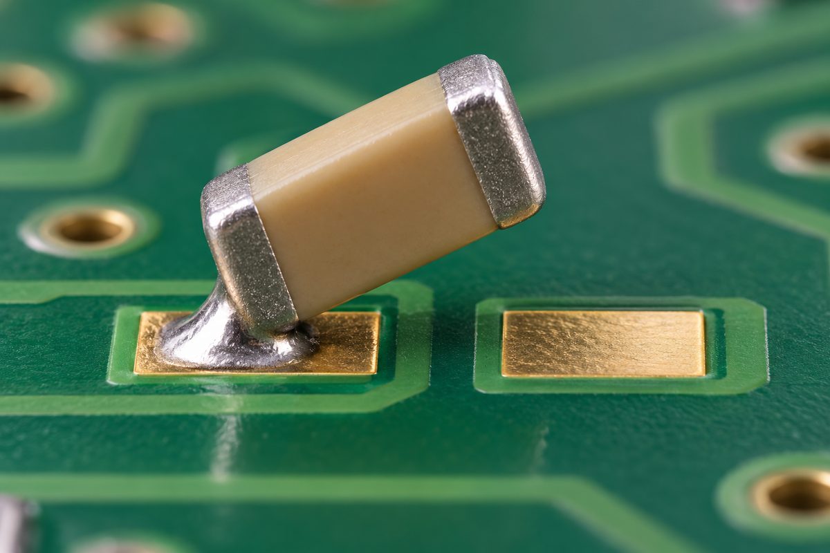
Small passives can reveal local differences between their two terminations. Unequal copper, paste, placement contact, and heating can contribute to tombstoning. A sensor placed several millimeters away may miss the specific imbalance, while the attachment itself can disturb a very small joint. Use careful measurement design and correlate thermal evidence with print and placement data.
The SMT tombstoning investigation guide explains why both ends should be compared before changing the oven. If direct junction measurements would be too intrusive, use a representative coupon or validated proxy and clearly state the limitation.
Do not tune the process around one defective reference without checking the full board. A slower conveyor or hotter zone may improve one cold joint while increasing oxidation, flux exhaustion, intermetallic growth, component exposure, or board deformation elsewhere.
How many thermocouples are enough?
There is no universal channel count. The number should cover the meaningful thermal extremes, package and material limits, panel positions, defect hypotheses, and customer requirements without creating unnecessary disturbance. A simple board may need only a few well-selected channels; a large mixed-mass assembly or panel may require more measurements or multiple runs.
If the profiler has limited channels, prioritize locations by consequence and uncertainty. Preserve a common reference channel when comparing runs, and change only a controlled subset when investigating additional sites. Multiple runs are comparable only when board condition, attachments, oven loading, conveyor direction, recipe, and other relevant variables remain controlled.
For an engineering quotation review, submit Gerbers, BOM, pick-and-place data, assembly drawings, panel details, solder paste, temperature-sensitive parts, quantities, and test or profiling requirements through the PCB assembly RFQ path. This lets profiling needs be evaluated with fabrication, sourcing, stencil, placement, and inspection plans.
How should profile data be evaluated?
Compare each channel with the applicable process window and component or material constraints. Typical metrics may include ramp behavior, soak behavior, time above the paste’s liquidus reference, peak temperature, and cooling behavior, but the exact definitions and limits must come from the selected materials and requirements. Do not combine numbers from different paste datasheets into a synthetic specification.
Look at the spread among channels as well as individual compliance. The process window must accommodate the coldest relevant joint without exceeding the hottest sensitive location. If there is no common window, changing oven settings alone may be insufficient. Design, copper balance, stencil, pallet, airflow, component selection, or assembly sequence may need review.
Record profiler identity, calibration status, thermocouple type, channel map, attachment method, board and panel revision, BOM variant, paste product and lot when required, oven, recipe, conveyor speed, loading, atmosphere, date, operator, raw curves, and approval. A screenshot without this context is difficult to reproduce.
When should a PCBA be re-profiled?
Re-profile when a change could alter product heating or when evidence shows the validated condition may no longer apply. Triggers can include board revision, copper or stackup change, panel change, component package or mass change, solder paste or alloy change, pallet or carrier change, oven maintenance, line transfer, altered loading, or a repeated thermal defect.
A BOM alternate can be electrically equivalent but thermally different. A connector supplier change may alter mass or finish. A shield added late in design can affect airflow. Use change control to decide whether documented review is enough or a new measured profile is required.
If a defect investigation needs a new profile, provide defect locations, X-ray or inspection evidence, current recipe, prior profiles, material changes, and quantities through the engineering review page. The goal is a scoped measurement plan, not an untraceable trial-and-error recipe.
Pre-release profiling checklist
- Map high-mass, low-mass, sensitive, and defect-related locations.
- Use a populated or demonstrably representative profiling assembly.
- Define what each channel measures and why it was selected.
- Attach welded junctions consistently and verify them after the run.
- Include expected cold and hot locations plus panel-position risks.
- Use current paste, component, laminate, and product limits.
- Evaluate channel spread, not only one passing curve.
- Record board, BOM, panel, recipe, loading, equipment, and calibration context.
- Define re-profile triggers under change control.
Good thermocouple placement turns an oven recipe into evidence about the actual mixed-mass assembly. Select sites from thermal risk, attach each junction to the intended interface, preserve measurement context, and protect both the coldest joint and hottest sensitive part. For a one-stop PCBA review, send the controlled fabrication package, BOM, placement data, paste requirements, quantities, and profile constraints through the RFQ page so PCB fabrication, component sourcing, SMT assembly, reflow validation, inspection, testing, and delivery can be planned together.
Technical references: Indium Corporation thermocouple attachment application note and AIM Solder thermocouple profiling guidance.
Latest Blog
Contact Info
Phone: +86-755-82882936
Email: [email protected]
WhatsApp: +86-13570802455
Wechat: +86-13570802455
Address: 2nd floor,D Bldg.,Electric Link Technology Bldg.,Gongming,Guangming New Dist.,518106 Shenzhen, China