
1-Layer PCB: Design, Cost, and Manufacturing Guide
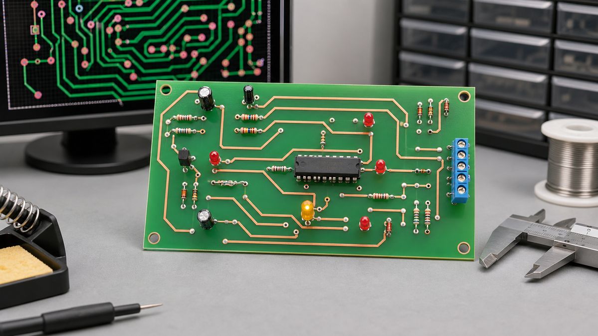
Table of Conent
Table of Conent
A 1-layer PCB is a printed circuit board with conductive copper on only one side of its insulating substrate. It is usually the most practical choice for simple, cost-sensitive electronics that do not require dense routing, controlled impedance, or complex power distribution.
Simple does not mean careless. A well-designed single-sided board can be reliable, easy to inspect, and economical at scale. A poor layout, however, can turn its routing limits into extra jumpers, assembly problems, and avoidable redesign work. This guide explains where a 1-layer PCB fits, how its construction affects performance, and what to check before releasing the design for fabrication.
Key Takeaways
- A 1-layer PCB carries all copper traces on one side of the substrate, which keeps fabrication straightforward.
- It works best for low-density circuits, through-hole assemblies, simple LED products, controls, and power boards.
- Component placement and routing must be planned together because traces cannot freely cross.
- Board material, copper weight, trace geometry, hole sizes, and solder mask all affect cost and reliability.
- Early DFM review helps confirm that the board can be fabricated and assembled without unnecessary jumpers or rework.
What Is a 1-Layer PCB?
A 1-layer PCB, also called a single-layer or single-sided PCB, has one conductive copper layer bonded to an insulating base material. Components may sit on the opposite side, particularly in through-hole designs, while their leads pass through drilled holes and solder to pads on the copper side.
The basic structure normally includes:
- A substrate that gives the board mechanical strength
- One copper foil layer that forms traces, pads, and copper areas
- Solder mask over the copper where protection is required
- Silkscreen markings for references, polarity, and assembly guidance
- A surface finish on exposed pads to preserve solderability
This construction is much simpler than a multilayer PCB, which uses internal copper layers and plated interconnections between layers. The simpler stackup reduces fabrication steps, but it also gives the designer less routing space.
Single-layer boards are available in several material systems. FR-4 is common when mechanical strength and electrical insulation matter. Paper-based phenolic laminates may suit very cost-sensitive consumer products. Aluminum-backed materials are used when heat from LEDs or power devices must move efficiently into a metal base.
The right material depends on operating temperature, mechanical load, electrical requirements, expected lifetime, and production volume. A low-cost laminate is not economical if it creates field failures or cannot tolerate the assembly process.
Where Does a Single-Layer PCB Work Best?
A 1-layer PCB is most effective when the circuit has a modest component count and a clear routing path. Typical applications include:
- LED lighting modules
- Power supplies and simple power distribution boards
- Relays, timers, and basic control circuits
- Household appliance controls
- Toys and low-complexity consumer electronics
- Sensor breakout boards
- Simple audio circuits
- Through-hole educational and prototype boards
- Automotive auxiliary modules with uncomplicated circuitry
These products benefit from a board that is easy to manufacture, inspect, repair, and reproduce. The visible routing also makes troubleshooting relatively direct.
A single-layer layout becomes less attractive when the circuit includes fine-pitch packages, high pin-count devices, high-speed buses, sensitive RF paths, dense connector arrangements, or several supply rails. In those cases, forcing the design onto one copper layer may increase board area and require many wire jumpers. A compact two-layer board can then be the more economical system-level choice.
Consider the full production cost rather than only the bare-board price. A larger 1-layer PCB with ten manual jumpers may cost more to assemble than a smaller 2-layer board with straightforward automated placement.
1-Layer PCB Advantages and Limitations
Advantages
The strongest advantage is manufacturing simplicity. With only one conductive layer, the fabrication sequence is shorter and alignment between multiple copper layers is not required.
Other practical benefits include:
- Lower bare-board cost for suitable designs
- Shorter and more predictable fabrication flow
- Straightforward visual inspection
- Easier fault finding and repair
- Broad availability from PCB fabricators
- Good suitability for through-hole components
- Lower technical risk for uncomplicated circuits
- Efficient panel utilization when the outline is compact
The design can also be highly robust. Wide traces, generous spacing, and accessible solder joints are often easier to achieve on a simple board.
Limitations
The routing area is restricted to one side. Two traces cannot cross unless the design uses a jumper, a zero-ohm resistor, a component lead, or a revised placement arrangement.
Additional limitations include:
- Lower routing density
- Larger board dimensions for complex circuits
- Limited ground and power distribution options
- More difficulty controlling return-current paths
- Poor fit for high-speed or high-frequency designs
- Greater dependence on careful component placement
- Possible manual assembly cost when jumpers are required
- Limited thermal spreading unless copper areas or a metal substrate are used
These trade-offs should guide the layer-count decision early. Changing from one layer to two after placement is complete often creates more work than selecting the correct architecture at the start.
How to Design a Reliable 1-Layer PCB
Start With Component Placement
Placement determines whether single-sided routing is practical. Put connectors, switches, displays, mounting holes, and mechanical interfaces first because their positions are usually constrained.
Then group related components by function. Keep decoupling capacitors close to device power pins. Place protection parts near the connector or power entry they protect. Orient resistors and diodes consistently where possible to simplify assembly and inspection.
Before routing, look for natural signal flow. A layout that follows input, processing, and output stages usually needs fewer crossings. Our guide to PCB layout design explains why placement decisions made at this stage affect the entire manufacturing process.
Route Power and Critical Nets First
Route high-current paths, sensitive analog signals, and critical timing connections before ordinary low-current signals. Give current-carrying traces enough width for the expected load, copper thickness, allowed temperature rise, and ambient conditions.
Do not select a trace width from habit. Calculate it from the electrical and thermal requirements, then confirm that it fits the fabricator’s capability. Pay special attention to narrow sections near pads, connectors, fuses, and switches.
Use broad copper areas where they improve current handling or heat spreading. Copper is the standard conductor because it combines electrical conductivity with practical fabrication characteristics; this overview explains why copper is used in circuit boards.
Manage Trace Crossings Deliberately
A clean single-layer board minimizes jumpers, but a jumper is sometimes the correct engineering solution. Treat every jumper as a real component with a reference designator, controlled length, assembly method, and inspection requirement.
Common crossing options include:
1. Repositioning or rotating components 2. Routing beneath compatible through-hole components 3. Using a zero-ohm resistor for automated assembly 4. Adding an insulated wire link 5. Increasing the board area 6. Moving to a 2-layer construction
Do not create awkward trace geometry solely to avoid one jumper. Long detours can increase resistance, noise pickup, and board size. Compare the electrical and assembly consequences.
Keep Return Paths Short
Even a low-frequency circuit needs a defined current return path. Avoid routing signals in a way that forces return current around large slots or long perimeter paths. Use connected ground copper where the layout allows it, and check that narrow necks do not divide the ground area into poorly connected sections.
For mixed-signal boards, keep noisy switching current away from sensitive analog sections. Physical separation and deliberate grounding matter more when there is no uninterrupted internal ground plane.
Design for Fabrication and Assembly
Set design rules from the selected manufacturer’s verified capability rather than copying generic minimum values. Confirm:
- Minimum trace width and spacing
- Minimum finished hole size
- Annular ring requirements
- Board thickness tolerance
- Copper weight tolerance
- Solder mask clearance
- Silkscreen-to-pad clearance
- Supported surface finishes
- Panelization and edge-clearance rules
Also check component footprints against the actual part drawings. Incorrect hole diameters and pad sizes are common causes of assembly delays in through-hole designs.
If the product will be assembled after fabrication, decide whether wave soldering, selective soldering, hand soldering, or reflow will be used. Component orientation, spacing, and thermal relief should support that process.
Materials and Specifications That Affect Cost
Substrate Material
FR-4 provides a useful balance of mechanical strength, insulation, moisture resistance, and availability. Paper phenolic materials can reduce cost in suitable low-stress products, while aluminum-backed boards help manage heat in lighting and power applications.
Material selection should follow the operating environment. Ask about temperature, humidity, vibration, flammability requirements, mechanical support, and expected product life before choosing the least expensive laminate.
Copper Weight
One-ounce copper is a common starting point, but it is not a universal rule. Higher current may require wider traces, heavier copper, or both. Heavier copper can affect etching tolerances, spacing requirements, and price.
Use a current-capacity calculation and review hot spots around terminals and power devices. If heat is a central design constraint, consider whether an aluminum-backed PCB or a different board architecture is more appropriate.
Board Thickness
A commonly available board thickness may reduce sourcing friction, but mechanical requirements should lead the decision. Connector fit, enclosure slots, stiffness, vibration, and handling all influence thickness.
Thin boards can flex during assembly. Thick boards may not fit edge connectors or mechanical guides. Include the finished thickness and tolerance in the fabrication documentation.
Surface Finish
The surface finish protects exposed copper and supports soldering. HASL is widely used for cost-sensitive designs, while flatter finishes can be helpful for certain component and process requirements. The best choice depends on pad geometry, storage time, assembly process, environmental restrictions, and budget.
Outline and Panelization
Unusual outlines, internal cutouts, narrow slots, and inefficient panel layouts can raise cost. Keep the outline practical and define tooling, breakaway rails, fiducials, and depanelization requirements with the assembler.
Panelization affects material utilization and assembly throughput. This guide explains how PCB panelization can improve efficiency and reduce cost.
The 1-Layer PCB Manufacturing Process
A typical fabrication flow starts with the approved Gerber and drill data. The manufacturer reviews the files for basic producibility, prepares the production panel, images the copper pattern, etches unwanted copper, drills the board, and applies solder mask, silkscreen, and surface finish as specified.
The exact sequence varies with material and factory process, but the core stages are:
1. Incoming material preparation 2. Copper pattern imaging 3. Development and etching 4. Drilling or routing 5. Cleaning and inspection 6. Solder mask application 7. Silkscreen printing 8. Surface finishing 9. Electrical testing 10. Profiling and final inspection
Single-sided boards still require disciplined process control. Etching must preserve trace geometry, drilled holes must align with pads, and the final finish must support reliable soldering.
Provide a complete fabrication package. At minimum, include copper data, solder mask, silkscreen, drill files, board outline, readme notes, material, finished thickness, copper weight, surface finish, quantity, and any testing requirement.
For assembly, also provide the BOM, centroid or placement data when relevant, assembly drawings, polarity information, approved substitutions, and test instructions.
How to Choose a 1-Layer PCB Manufacturer
A suitable manufacturer should do more than quote the board. Ask whether the team reviews trace spacing, annular rings, drill sizes, board edge clearance, solder mask, and manufacturability before production.
Evaluate these points:
- Experience with your selected substrate
- Supported board dimensions and tolerances
- Copper and surface finish options
- Electrical testing coverage
- Traceability and quality documentation
- Prototype and production capacity
- Assembly support when required
- Responsiveness of engineering communication
- Handling of panelization and special outlines
- Clear process for resolving DFM questions
For a custom design, the choice also depends on whether the supplier can support revisions and production growth. Our comparison of custom PCB and standard PCB approaches can help frame that decision.
Send the same controlled data package to every supplier you compare. Quotes based on different materials, testing levels, tolerances, or lead times are not directly comparable.
When Should You Move to a 2-Layer PCB?
Move beyond a 1-layer PCB when routing compromises begin to dominate the design. Warning signs include numerous jumpers, an expanding outline, broken return paths, thermal congestion, poor access for assembly, or difficulty separating noisy and sensitive circuits.
A 2-layer board adds routing freedom and can support a more continuous ground structure. Although its bare-board price may be higher, it can reduce board area, jumper count, assembly labor, and redesign risk.
Make the decision using total delivered cost:
- Bare PCB fabrication
- Component and jumper cost
- Assembly time
- Inspection effort
- Test coverage
- Rework risk
- Enclosure size
- Expected production volume
For a simple LED controller or relay board, one layer may remain the best answer. For a microcontroller board with dense connectors and several interfaces, two layers will usually produce a cleaner result.
Final 1-Layer PCB Checklist
Before releasing the files, verify:
- The circuit is genuinely suitable for single-sided routing
- All footprints match component drawings
- Trace widths support the required current
- Spacing follows the manufacturer’s rules
- Return paths are short and connected
- Jumpers are documented as components
- Hole and annular ring sizes are manufacturable
- Solder mask openings are correct
- Silkscreen does not cover exposed pads
- Board edge and mounting clearances are adequate
- Fabrication notes match the Gerber data
- BOM and assembly drawings use the latest revision
- Electrical test requirements are defined
- Panelization supports the planned assembly process
A 1-layer PCB is a strong engineering choice when the circuit, mechanics, and production method all support it. Keep the layout direct, verify the current and thermal requirements, and involve the manufacturer before small uncertainties become production delays.
AssyPCB supports PCB fabrication and assembly from prototypes through production. Upload your Gerber files and BOM to request a quote and receive DFM feedback for your 1-layer PCB project.
Latest Blog
Contact Info
Phone: +86-755-82882936
Email: [email protected]
WhatsApp: +86-13570802455
Wechat: +86-13570802455
Address: 2nd floor,D Bldg.,Electric Link Technology Bldg.,Gongming,Guangming New Dist.,518106 Shenzhen, China