
PCB Test Point Design: Probe Access and Production Release Checks
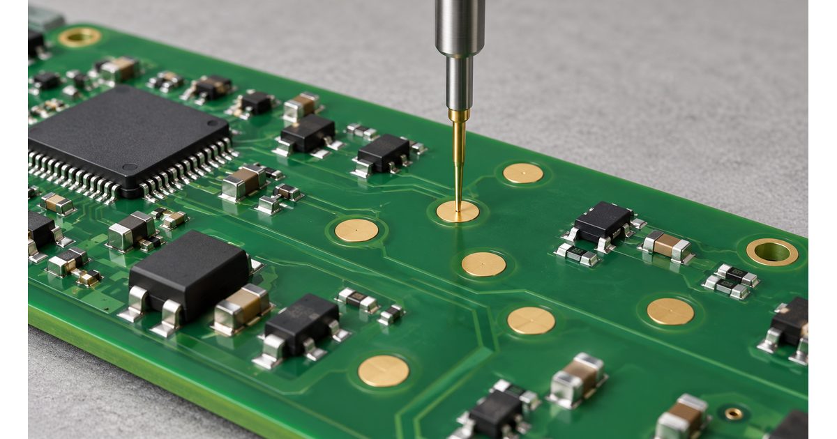
Table of Conent
Table of Conent
PCB test point design gives test equipment a practical way to contact selected circuit nodes. A useful test point must be electrically appropriate, physically reachable at the required production stage, and clearly identified in the released data. Adding exposed copper alone does not establish a complete test strategy.
The most expensive access problems often appear after component placement, fixture planning, or enclosure decisions. A pad visible in the bare-board layout may be hidden on the assembled product. Plan test access with the assembly and test teams before release, then verify the actual exported package rather than relying only on a CAD marker.
Start with the test objective
Identify what each planned test is meant to detect or measure. Bare-board continuity and isolation checks, assembled-board structural tests, firmware programming, powered functional tests, and engineering debug have different access requirements. One test point may support several activities, but that compatibility needs review.
A test-access list should connect each node to a purpose. Include the net name, board side, coordinate, contact geometry, expected test stage, and any restrictions on applying power or signals. Record reference returns and programming connections alongside signal nodes so the test engineer can evaluate the complete connection.
Separate required access from convenience access. A debug pad that helps an engineer inspect a prototype is not automatically suitable for repeated production contact. Conversely, a production fixture pad may be inaccessible after an enclosure is installed. State which product condition applies to each requirement.
Distinguish bare-board access from assembly access
Altium’s testpoint-assignment documentation treats fabrication and assembly access separately. That distinction matters because components can obstruct sites that were available before population. A fabrication test designation should not silently become an assembly test designation.
Review the populated board, not just the copper layers. Account for connectors, component bodies, mechanical hardware, shields, adhesives, and later process steps. Include the actual BOM variant because a location accessible on one configuration may be covered on another.
Use the assembly process and quality-control guide to place access requirements within the manufacturing route. Define whether contact occurs before coating, after programming, before final enclosure assembly, or at another agreed stage. An otherwise valid pad can become unusable when the process order changes.
Agree on the probing method before setting dimensions
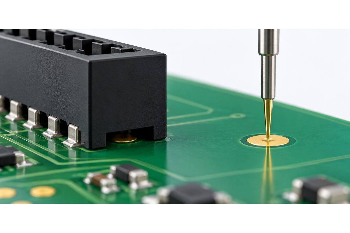
A dedicated spring-probe fixture and a moving-probe system impose different mechanical constraints. Manual probing adds operator access and handling concerns. Confirm the intended method, board side, support arrangement, and contact approach before adopting a pad-size or spacing rule from another project.
Ask the test provider for the complete access envelope: usable contact diameter, adjacent-point spacing, component clearance, edge clearance, positioning tolerance, and any fixture-grid requirements. These values depend on equipment and fixture design. There is no single dimension that guarantees compatibility with every assembly test system.
Altium’s testpoint-rule documentation includes separate controls for physical size, spacing, component and board-edge clearance, permitted sides, and grid use. Translate agreed supplier requirements into the appropriate design checks. A default rule is a starting configuration, not proof of production suitability.
Need an access review before layout freeze? submit the PCB layout outputs, populated assembly drawings, intended test method, required nodes, quantities, and mechanical constraints for engineering and quotation review. Include unresolved access exceptions so they can be evaluated before fabrication.
Design a stable contact surface
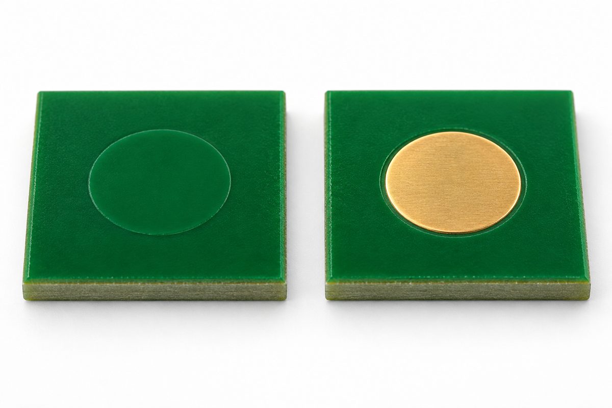
The probe needs a conductive surface it can actually reach. Review the exposed area after solder-mask processing and any assembly materials are applied. A copper feature assigned as a test point in CAD can still be covered by mask, coating, adhesive, or a component.
Use the solder-mask opening and release guide when reconciling copper geometry with the final mask artwork. Confirm that the intended opening survives the output process and meets the agreed fabrication constraints. Do not infer the finished opening from the copper-pad diameter alone.
Via-based contact needs particular care. A tented via blocks direct contact, while an open via presents a different surface from a solid pad. Hole geometry, finish, probe-tip style, and possible residue affect the contact approach. Ask whether the selected location is accepted rather than assuming every exposed via is interchangeable with a dedicated pad.
Keep legends and nearby features out of the agreed contact area. Define how a contact-quality problem will be distinguished from a circuit failure during test development. Repeated retesting without understanding unstable contact can mask a fixture or access issue instead of confirming product quality.
Review the assembled three-dimensional clearance
A clear top-down gap does not necessarily leave room for a probe body. Check the probe’s approach direction and its full mechanical envelope against tall components, connector latches, shield walls, and nearby hardware. Evaluate the product at the stage when testing will occur.
For fixture-based contact, review how the board is located and supported. The fixture must keep the required contact alignment without relying on an unsupported board bending into position. Discuss support locations, sensitive components, and any restrictions on loading with the fixture designer.
Board-versus-panel testing also changes access planning. Rails, repeated board images, rotated instances, and temporary tooling can affect the fixture reference system. Define whether the test program addresses individual boards or a panel, and reconcile the coordinates with that physical configuration.
A hypothetical example is a pad that passes a two-dimensional clearance check but sits beneath a connector latch on the assembled variant. Moving the pad may solve access, but it also changes the fixture and exported coordinates. Treat the correction as a controlled design revision, not an undocumented shop-floor workaround.
Protect circuit behavior while adding access
Test access is part of the electrical design. An added pad, branch, or via changes the connected geometry. On a sensitive signal, the access structure or attached probe can affect the quantity being measured. Review the relevant circuit requirements before adding convenient branches or enlarging copper.
For high-speed, RF, low-level analog, or high-impedance nodes, agree on an appropriate measurement interface and return path with the responsible engineer. Do not apply a generic production-pad pattern to every net. Some requirements may be better addressed through a connector, boundary-scan strategy, or another approved method.
Powered test access also requires a defined operating state. Document intended supply connections, returns, programming states, and restrictions on external drive. Fixture contact sequencing and test procedure must be reviewed for the actual circuit; a placement file cannot communicate all these electrical conditions.
Measure coverage by the planned tests, not pad count
Physical access enables tests but does not guarantee that each relevant defect can be detected. Record which requirements are addressed by structural testing, optical inspection, programming checks, and powered functional testing. Identify gaps rather than presenting a large number of test points as complete coverage.
Keysight’s in-circuit testing overview describes how access, fixture design, and complementary methods influence manufacturing test coverage. Use a project-specific coverage review to decide what is practical. Equipment marketing or a generic method description is not evidence of the coverage achieved on a particular board.
Distinguish an inaccessible node, an accessible node with no implemented test, and a tested function with a known detection limit. Those are different engineering decisions. Assign an owner to unresolved requirements and keep approved exceptions with the production release.
For a variant or mixed-test build, send the BOM variants, access list, test requirements, programming needs, quantities, and accepted coverage exceptions for a manufacturing and quotation review. State the required outcome rather than requesting an undefined “full test.”
Release a consistent test-data package
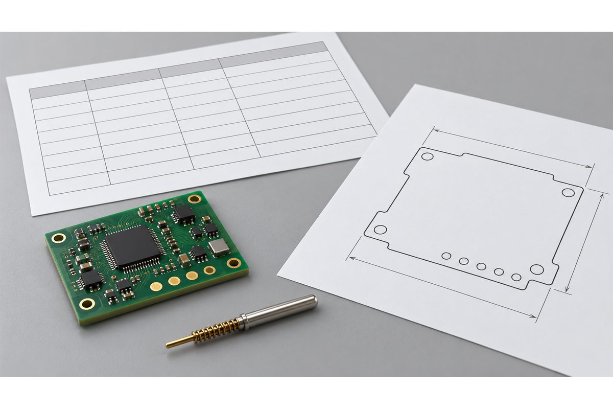
Provide the net and test-point list, coordinates, units, origin, board side, assembly drawings, BOM variant, and revision identity in an agreed format. Reconcile the list with the actual layout exports. Stable identifiers help the test engineer connect geometry to circuit intent without guessing from a screenshot.
Discuss the package with the SMT assembly service team alongside the fabrication and assembly files. Confirm project-specific test availability and deliverables rather than assuming a general assembly service includes every fixture, program, or measurement method.
After changes to placement, pad geometry, coating, panelization, or variants, repeat the affected access checks and coordinate review. Preserve the approved test and fixture revision relationship. A correct old fixture can become incorrect when used with an updated board.
Pre-release checklist
- Define each test objective and the product stage at which access is needed.
- Confirm the probing method and supplier-specific geometry requirements.
- Check populated variants, contact surfaces, approach envelopes, and support.
- Review electrical loading and powered-test restrictions.
- Identify actual coverage gaps and accepted exceptions.
- Reconcile coordinates and identifiers with one controlled release revision.
Good PCB test point design connects the circuit, assembled geometry, and test procedure. Resolve access early, verify the exported data, and keep coverage claims tied to implemented tests.
Preparing production files? submit the fabrication package, BOM, assembly drawings, test-point list, test requirements, quantities, and revision notes for engineering review and quotation. Include the intended test stage and unresolved constraints.
Latest Blog
Contact Info
Phone: +86-755-82882936
Email: [email protected]
WhatsApp: +86-13570802455
Wechat: +86-13570802455
Address: 2nd floor,D Bldg.,Electric Link Technology Bldg.,Gongming,Guangming New Dist.,518106 Shenzhen, China