
PCB Solder Mask Design: Openings, Dams, and Release Checks

Table of Conent
Table of Conent
PCB solder mask design determines which copper areas remain exposed and where protective mask remains between features. A layout can have acceptable copper spacing yet produce unsuitable mask openings or fragile mask bridges. The practical review therefore needs copper geometry, package requirements, registration allowance, and the fabricator’s actual process rules together.
This guide focuses on release decisions for engineers and buyers: how to distinguish openings from copper pads, evaluate the remaining mask between them, preserve package-specific pad definitions, and resolve manufacturing edits before ordering. It does not prescribe one expansion value, one minimum dam width, or one color-dependent capability for every supplier.
Separate copper, solder mask, and paste outputs
A copper pad, its solder mask opening, and its solder paste aperture are different design features. Changing one does not mean that the others should change automatically. Keep their purpose and exported geometry separate during footprint review.
Altium’s mask-rule documentation describes expansion or contraction of mask geometry and treats solder mask and paste mask as separate rule categories. It also identifies individual-object overrides. Verify the actual generated openings rather than assuming a board-wide rule describes every pad.
The SMT stencil guide provides context for paste deposition. A solder mask revision is not a substitute for stencil design, and a paste-aperture adjustment should not silently alter exposed copper or package land definition.
When reviewing manufacturing files, confirm layer names, orientation, and the meaning of the shapes shown in the viewer. Do not approve a mask layer based only on its display color. Ask which shapes represent openings and inspect them against the copper beneath.
Understand expansion as a geometric instruction
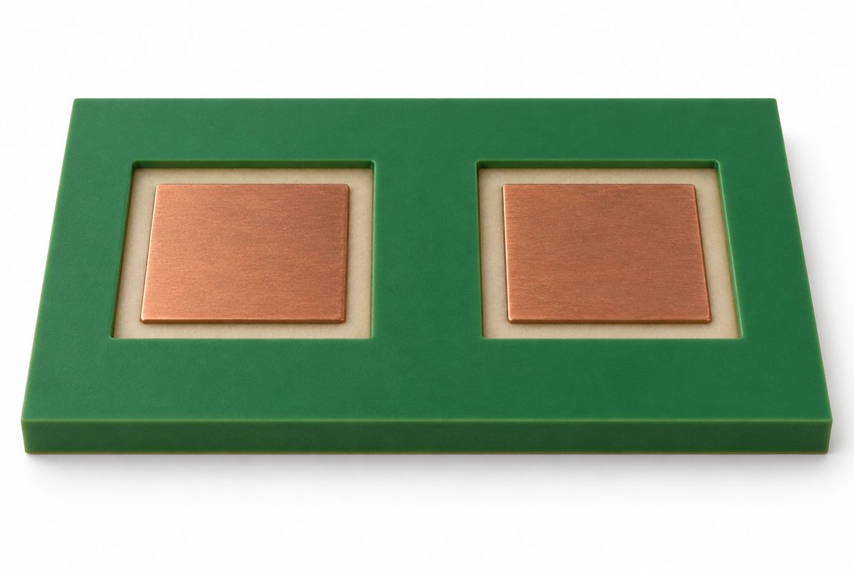
For a pad-edge-based rectangular opening with equal positive expansion on opposite sides, the opening dimension increases by twice the per-edge expansion. This is a geometry relationship, not a recommended manufacturing value. Confirm the reference used by the CAD rule, particularly where a tool can calculate from a hole instead of the copper land.
Positive expansion can provide clearance around a copper pad; reducing that clearance changes the relationship between the pad and mask. Do not choose an expansion simply because it removes a design-rule warning. Check the package requirements and manufacturing agreement first.
Keep top and bottom requirements explicit where they differ. Review custom-shaped openings, footprint-level settings, and pad or via overrides in the exported data. A clean rule summary cannot compensate for a local object that was configured differently.
Send your PCB files, package land-pattern requirements, and solder mask constraints for a manufacturing quote review. Identify critical fine-pitch locations so opening and registration questions can be discussed before release.
Evaluate the remaining mask, not only pad spacing
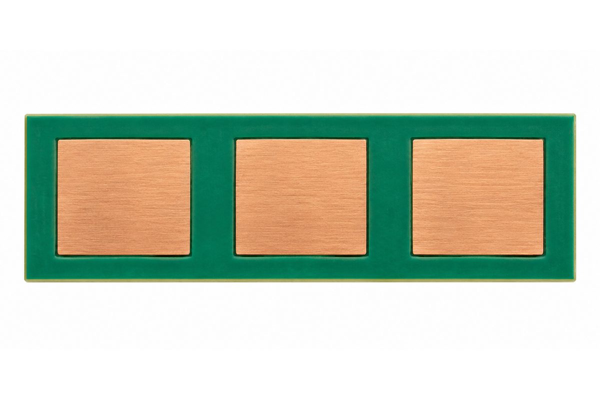
A mask dam, web, or sliver is the remaining mask between adjacent openings. It is not the copper-to-copper clearance. Evaluate it alongside the clearance from an opening to nearby copper that should remain covered.
Eurocircuits’ soldermask design guidance distinguishes opening clearance, remaining webs, and overlap to neighboring copper. Its published values are tied to its own production process. Use that framework to ask your fabricator for applicable rules rather than importing those values as AssyPCB capabilities.
Larger neighboring openings leave less mask between them. If the remaining web is unsuitable for the selected process, the review must resolve both exposed-pad requirements and the remaining-mask requirement. Neither should be silently sacrificed to make the other pass.
Example: expansion reduces a straight web
For illustration only, consider two parallel copper-pad edges separated by 0.18 millimeter. If each opening expands 0.05 millimeter into that gap, the nominal remaining web is 0.08 millimeter. These hypothetical numbers are not fabrication recommendations or acceptance limits.
The simplified calculation assumes pad-edge-based expansion and straight opposing edges. It excludes registration variation and other geometry. The result must still be reviewed against the agreed process and package requirements. Increasing the expansion would reduce the web further; decreasing it would increase the web but change the pad-to-mask clearance. This is why one warning cannot be resolved independently of the surrounding design.
Preserve the package’s pad definition
For non-solder-mask-defined (NSMD) pads, the opening leaves the copper-pad boundary exposed. For solder-mask-defined (SMD) pads, mask overlaps part of the copper and defines the exposed area. These are intentional land-pattern choices, not interchangeable ways to clear a sliver warning.
AMD’s BGA layout guidance explains the distinction and recommends NSMD pads for the devices addressed by that guide. Apply the relevant component manufacturer’s guidance to your actual package; do not turn one manufacturer’s recommendation into a universal rule for every component.
Review a proposed change from NSMD to SMD, or vice versa, as a package land-pattern change. Involve the responsible design and assembly reviewers. Do not let a fabricator’s geometry adjustment unintentionally change the approved exposed-pad area.
If a shared opening is proposed for closely spaced pads, identify exactly which features it includes and obtain the necessary review. A merged opening should be a documented decision, not an unexplained difference between the CAD model and production artwork.
Agree process limits before changing CAD rules
Ask the supplier to confirm the applicable mask process, registration allowance, minimum manufacturable web, and treatment of features below that web requirement. Record what the quoted limits refer to: input artwork, resulting mask geometry, or a finished-board acceptance condition.
Confirm whether the selected mask material or color changes the quoted manufacturing rules. Do not assume that a setting approved for one process applies unchanged to another. Equally, do not claim that one color is always better without a product-specific reason and verified process information.
If the supplier proposes removing a narrow web, reducing an opening, or changing a special feature, request an annotated comparison. It should identify the location, original geometry, proposed geometry, and the manufacturing reason. Keep approvals tied to the board revision.
Request a DFM and quotation review with annotated critical mask features and permitted-change notes. Include the component package requirements so fabrication and assembly constraints can be considered together.
Review special exposed and covered features explicitly
Identify connector contacts, test access, fiducials, mechanical contact areas, and any copper that must remain exposed. Review nearby mask openings rather than relying only on ordinary component-pad rules. A test-point requirement can be defeated by an overlooked local mask setting.
Specify the intended treatment of vias separately. A CAD tenting instruction does not, by itself, establish a guaranteed physical closure or a filled-and-capped structure. Confirm the actual manufacturing arrangement where closure or surface condition matters to the application.
Check intentional mask-free regions against the drawing and assembly needs. Do not remove mask broadly as a shortcut for resolving crowded geometry. The approved footprint and manufacturing files should explain why those regions are exposed.
Check the exported release package
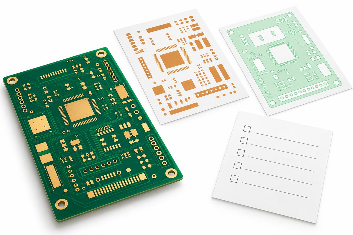
The PCB design-to-manufacturing checklist supports a controlled file handoff. Inspect the exported mask layers with copper and drill data, not only the native design view. Confirm both board sides and the final revision after local overrides or approved changes.
Review critical features at a useful zoom level and retain annotated approval images where they clarify the decision. Screenshots support communication but should not replace the actual manufacturing files. The supplier must receive the controlled data that the images describe.
Do not resolve a local fine-pitch issue by shrinking every opening on the board without reviewing the wider effect. Scope the change deliberately, recheck the affected features, and regenerate the complete controlled package.
Example: a local override survives a global change
Consider a hypothetical design in which the engineering team changes the board-wide expansion rule after a manufacturing review. One imported footprint still carries a manual pad override, so its exported openings remain unchanged. The updated rule table looks correct, but the released geometry does not match the intended revision. This is an illustrative example, not an AssyPCB production case.
The reviewer checks the affected footprint properties, compares the regenerated output with the approved copper, and confirms the local correction before release. The same check is then applied to other deliberately overridden features, without assuming every override is an error. Some may preserve valid package requirements. The lesson is to verify the resulting geometry and the reason for each exception, rather than trusting a global setting or deleting all overrides indiscriminately.
Make the purchase note specific
Supply the fabrication files, mask specification, component land-pattern requirements, critical-feature annotations, and agreed process constraints. State which edits are permitted and which require approval. Identify any special exposed regions or via treatment that cannot be inferred safely from ordinary footprints.
The published PCB manufacturing capabilities are a starting point for project discussions. Confirm the mask rules for the actual construction and quotation instead of treating a general capability page as approval of every fine-pitch feature.
Submit your PCB files and solder mask requirements for a project-specific quote. Clear opening geometry, realistic web requirements, and controlled release checks help engineering and purchasing resolve manufacturability questions before they become shipment disagreements.
Latest Blog

Contact Info
Phone: +86-755-82882936
Email: [email protected]
WhatsApp: +86-13570802455
Wechat: +86-13570802455
Address: 2nd floor,D Bldg.,Electric Link Technology Bldg.,Gongming,Guangming New Dist.,518106 Shenzhen, China