
QFN Solder Voiding: Connect X-Ray Results to the Build Process
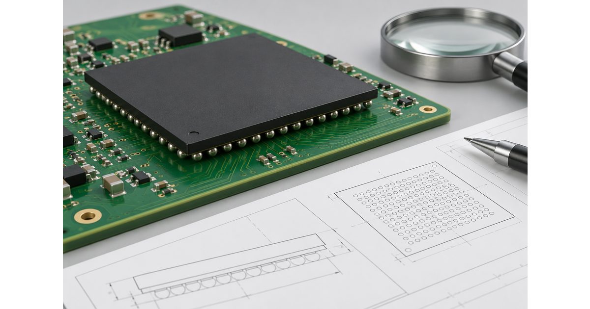
Table of Conent
Table of Conent
QFN solder voiding is the presence of gas pockets or unfilled areas within the reflowed solder layer, most often beneath the exposed thermal pad. An X-ray image can show their projected location and area, but it does not by itself prove root cause or product risk. A useful review connects the image to the package drawing, land pattern, stencil design, thermal-via construction, solder-paste record, placement data, and measured reflow profile. Acceptance must come from the product’s documented requirements and applicable component guidance, not from a universal percentage borrowed from another design.
This guide shows engineers and buyers how to turn an X-ray finding into a controlled disposition and a focused process investigation for prototype or production PCB assembly.
What does a QFN X-ray actually tell you?
A two-dimensional X-ray is evidence of projected density. It can reveal the overall soldered region, large or clustered voids, solder loss into vias, bridging, and gross placement offset. It normally cannot establish the three-dimensional shape, depth, or exact interface of every feature. Keep the inspection method, scale, orientation, threshold settings, and component reference with the record.
Confirm the exact package and exposed-pad function before interpreting the image. QFN variants differ in body size, terminal construction, thermal-pad geometry, pitch, and supplier recommendations. The pad may provide heat transfer, electrical grounding, mechanical anchoring, or a combination. Those functions determine whether void location matters as much as total projected area.
Why can the same void percentage have different consequences?
Void percentage alone is not a complete risk measure. A large void beneath a heat-generating die region may affect the thermal path differently from several small voids near the perimeter. A clustered pattern beside open thermal vias can indicate solder loss, while a fine distributed pattern may point toward gas-release behavior. Package power, duty cycle, board thermal design, pad function, product environment, and reliability target all shape the engineering judgment.
| Evidence | Question it can answer | Important limitation |
|---|---|---|
| 2D X-ray | Where are projected voids, bridges, or solder-loss patterns? | It compresses depth into one image. |
| Package guidance | What land, paste, via, and pad guidance applies? | Recommendations may be package-family specific. |
| SPI record | Was paste volume and alignment stable before placement? | It does not show reflow gas behavior. |
| Measured profile | Was thermal history consistent with the approved process? | One thermocouple may not represent every QFN site. |
| Cross-section or CT | What is the three-dimensional geometry at a selected site? | It is more costly and may be destructive. |
Which design inputs should be reviewed first?
Start with the component manufacturer’s current drawing and assembly guidance, then compare it with the released footprint. Analog Devices recommends segmented thermal-pad stencil openings rather than one large opening for many QFN packages because the pattern can help manage paste and gas escape. Its guidance also gives package-specific paste-coverage information, so the exact part must be checked. Texas Instruments documents how thermal-via size, location, and stencil openings can affect solder loss and voiding. These are design inputs, not universal acceptance rules.
Review copper-pad size, solder-mask definition, aperture pattern, stencil thickness, aperture area ratio, and any step-stencil feature. Then examine thermal vias. Open, tented, plugged, capped, or filled vias behave differently during reflow. If via-in-pad is used, the fabrication note must match the assembly assumption. The via-in-pad design guide explains why fill and planarization requirements need to be explicit.
Also check the thermal connection below the pad. Plane size, copper distribution, via connections, board thickness, and nearby high-mass features influence heat flow. A profile developed on another revision or panel configuration may not reproduce the same package temperature.
How do you connect the X-ray pattern to stencil printing?
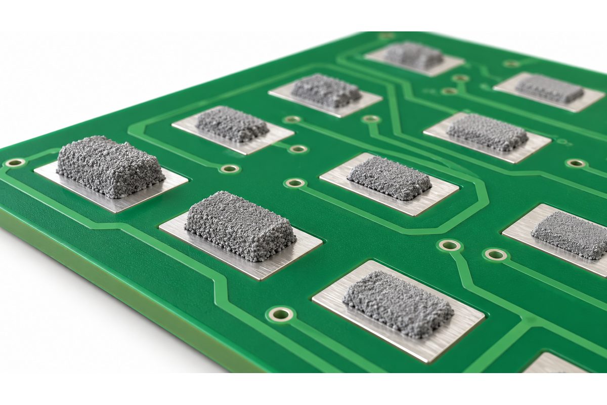
Compare the void map with the intended stencil window pattern and SPI results. Repeating features aligned with apertures suggest that paste segmentation, deposit balance, or gas escape deserves review. Random changes across similar sites may lead the investigation toward paste handling, printing stability, placement, contamination, or thermal variation.
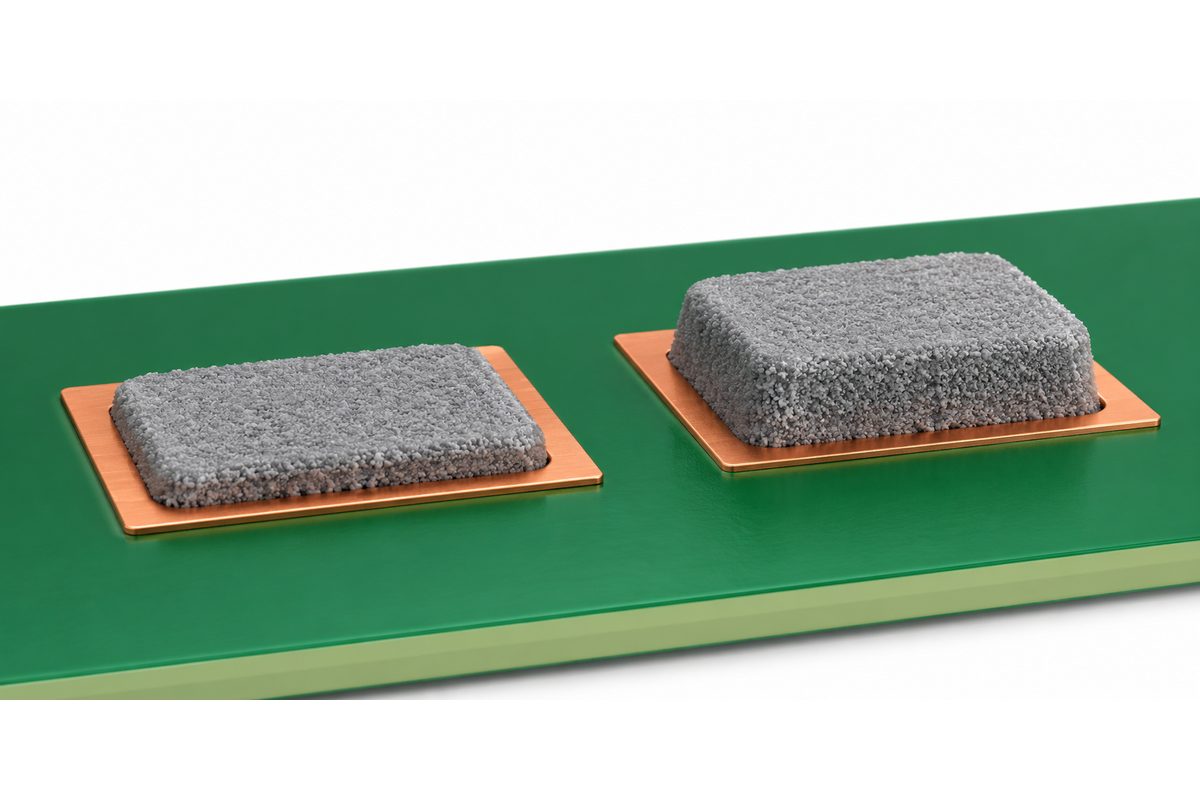
Use SPI trends rather than a single pass/fail result. Volume, area, height, offset, and panel location show whether deposits were stable. Review underside-wipe intervals, stencil condition, board support, squeegee parameters, paste exposure time, and replenishment records. Do not increase or decrease paste blindly: exposed-pad paste also changes package standoff, perimeter-joint geometry, solder beading, and movement. The solder paste inspection guide provides a framework for connecting deposits with downstream evidence.
How should placement and reflow evidence be reviewed?
Confirm component orientation, placement coordinates, rotation, package data, pickup behavior, and placement height. Excessive force can displace paste; insufficient seating or package warpage can change contact. Compare affected references with unaffected QFNs of the same package and their panel positions. A repeated edge, corner, or oven-lane pattern is more informative than an isolated percentage.
Use a measured profile from the relevant assembly, not only the oven recipe. Record thermocouple attachment and location, peak temperature, time above liquidus, ramp behavior, soak region, and repeatability as applicable to the paste supplier and component limits. A longer soak or higher peak is not automatically the solution. It can increase intermetallic growth, damage heat-sensitive parts, or create new defects. Evaluate one controlled change at a time and inspect the complete assembly afterward.
For a new build, send Gerbers, BOM, pick-and-place data, assembly drawings, QFN part numbers, acceptance notes, quantity, and test requirements through the PCB assembly quotation path. This lets the stencil, thermal pad, sourcing, process plan, inspection, and test scope be reviewed together.
When are extra inspection methods justified?
Escalate when existing evidence cannot support the product decision. Oblique X-ray views can separate overlapping features. Computed tomography provides a three-dimensional view for selected samples. Cross-sectioning confirms interface geometry at a specific location, but it is destructive and represents only that site. Thermal testing may be appropriate when the pad is central to heat removal, while electrical or functional tests address behavior defined by the test plan.
Do not let a passing functional test erase a manufacturing concern. A short bench test may not reproduce full power, temperature cycling, vibration, or service life. Conversely, a dramatic X-ray does not automatically prove an unreliable joint. Define the question first, then choose the method that can answer it.
How should you disposition an affected lot?
Separate immediate lot control from root-cause work. Identify the affected part number, references, board revision, assembly lot, panel positions, and inspection sample. Preserve representative units and original records. Apply the product drawing, customer specification, component guidance, and approved workmanship criteria. If the requirement is ambiguous, obtain a documented engineering decision instead of creating an informal shop-floor limit.
- Contain: isolate the defined population when the finding may affect requirements.
- Characterize: record location, distribution, projected-area method, sample size, and related defects.
- Compare: examine good and suspect units by reference, panel position, paste lot, stencil, line, and profile.
- Assess risk: connect the pad’s thermal, electrical, and mechanical functions to the product environment.
- Approve: document use-as-is, rework, additional screening, or rejection with the responsible authority.
QFN rework is not neutral. Local heating, pad damage, component moisture, solder volume, alignment, and cleaning access all require controls. A repaired board should receive the inspection and functional coverage defined for that repair.
How can a focused trial identify the real driver?
Build the trial around a hypothesis. If evidence suggests solder loss into open vias, compare one controlled via treatment or aperture arrangement while holding paste, profile, and placement constant. If the pattern follows deposits, compare a justified stencil change and review SPI before reflow. If it follows panel location, verify support, thermal loading, oven lane, and measurement placement. Changing stencil, paste, profile, and via design together prevents attribution.
Define success before the trial: X-ray method, sample size, allowable process window, perimeter-joint checks, electrical or thermal tests, and other defects that must not increase. Retain baseline and trial records under revision control. If a design change is approved, release the land pattern, fabrication notes, stencil data, assembly drawing, and inspection criteria together.
What should be included in the RFQ and build package?
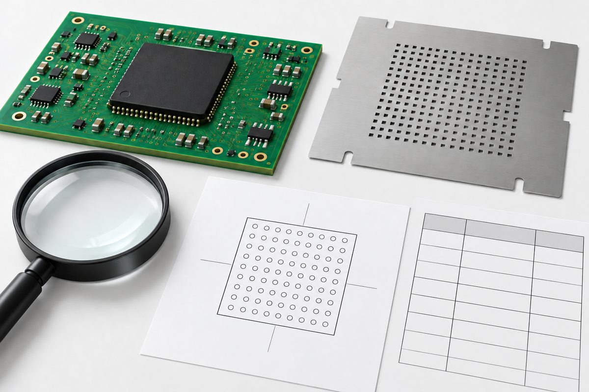
Include fabrication data, stackup and via requirements, BOM with manufacturer part numbers, centroid data, assembly drawings, substitutions, quantity, panel information, alloy restrictions, inspection criteria, test requirements, and relevant component notes. Identify any thermal pad whose function is safety-, power-, or reliability-critical.
For prototypes, ask what evidence will return with the first build: SPI summaries, measured profile, X-ray images and measurement method, first-article results, material traceability, and test records as appropriate. This turns the prototype into process learning. The pick-and-place file guide describes the broader path around printing, placement, reflow, and inspection.
If you already have an X-ray finding, submit the image, reference, board revision, package datasheet, stencil information, via construction, paste data, profile, quantity, and acceptance requirement through the quote request page. Engineering can then distinguish missing evidence from a true design or process change before a quotation or rebuild plan is finalized.
Practical pre-release checklist
- Exact QFN package drawing and revision confirmed.
- Exposed-pad electrical and thermal functions documented.
- Land pattern, solder mask, stencil, and vias reviewed together.
- SPI and placement evidence tied to references and panel positions.
- Measured profile tied to the actual assembly configuration.
- X-ray method, threshold, scale, orientation, and sample size recorded.
- Acceptance linked to a requirement or approved engineering disposition.
- Trial changes limited, traceable, and checked for unintended defects.
- Gerbers, BOM, centroid data, drawings, test scope, and quantities controlled.
QFN voiding is best managed as a connected design-and-process problem. X-ray locates the evidence; package guidance, footprint, stencil, vias, materials, placement, thermal history, and product requirements explain what it means. For a one-stop PCB assembly review, provide the complete data set through the RFQ page so fabrication, component sourcing, SMT assembly, inspection, and testing can be evaluated as one build.
Technical references: Analog Devices QFN design and assembly guidance and Texas Instruments QFN layout guidelines.
Latest Blog
Contact Info
Phone: +86-755-82882936
Email: [email protected]
WhatsApp: +86-13570802455
Wechat: +86-13570802455
Address: 2nd floor,D Bldg.,Electric Link Technology Bldg.,Gongming,Guangming New Dist.,518106 Shenzhen, China