
Via-in-Pad PCB Design: Filling, Capping, and BGA Escape
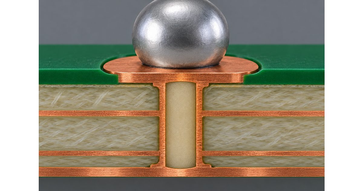
Table of Conent
Table of Conent
Via-in-pad places a via inside a component land instead of connecting the land to a separate via with a short trace. It can create valuable routing space around a dense package, but it also changes the fabrication and assembly requirements. The important decision is not simply where to place the hole. It is how the finished pad will support the solder joint and how the via construction will be specified and verified.
This guide focuses on defining a manufacturable via-in-pad structure for a production release. It separates filling, capping, and surface covering, explains the questions to resolve with the fabricator, and provides a practical RFQ and inspection framework. Numerical limits must come from the applicable design, purchase specification, and qualified manufacturing process.
Start with the routing problem you need to solve
For a BGA, escape routing connects the package lands to the rest of the board. A conventional approach may use a short trace from the land to a nearby via, often described as a dog-bone fanout. Via-in-pad moves that connection into the land area. Whether it is useful depends on pitch, pad geometry, trace and spacing rules, layer functions, and the available routing channels.
Evaluate the complete escape region rather than a single pad in isolation. Identify which nets need a layer transition and which can be routed without a via in the land. A selective approach may be appropriate, but the supplier still needs an unambiguous way to identify every feature requiring special processing.
Do not assume via-in-pad automatically means a particular layer count or HDI construction. The pad location and the via’s layer span are separate attributes. A through-via in a pad and a blind microvia in a pad need different construction details and may involve different production routes.
Distinguish covering, filling, and capping
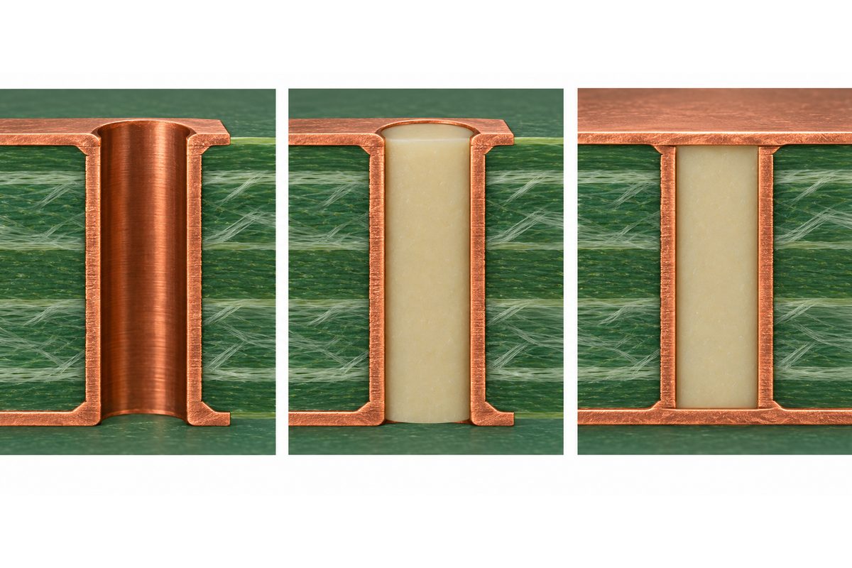
A covered opening is not the same as a filled barrel, and a filled barrel is not necessarily a metalized soldering surface. The IPC-4761 public contents and scope distinguish via-protection types, including filled, filled-and-covered, and filled-and-capped constructions. Use clear construction language with the applicable specification rather than relying on an unexplained abbreviation.
For solderable via-in-pad features, the land must be reviewed as part of the assembly interface. NCAB’s capped-via explanation describes a metalized cap over a filled hole and relates filled-and-capped structures to via-in-pad and BGA applications. This explains the terminology; it does not establish another supplier’s process limits.
State whether the requirement is a fill, a cap, a surface cover, or a defined combination. Avoid a drawing note that only says “plug vias” when the assembly depends on a planar solderable land. Ask the fabricator to confirm how it interprets the note before accepting a quotation or releasing the files.
Explain why an open via in a pad needs review
The referenced IPC-4761 contents identify filled-and-capped construction as Type VII. Confirm the agreed product and procurement requirements for the order; a via-protection term alone is not a complete acceptance specification.
An exposed hole inside a land can provide a path for solder or other process materials. Eurocircuits discusses these concerns and the purpose of filled, capped surfaces in its via-covering overview. The assembly result depends on the actual construction, land geometry, and soldering process; it should not be evaluated from a layout screenshot alone.
If a design uses an open via in a component pad, ask the assembler to assess that specific feature. Do not try to compensate by adding an arbitrary amount of solder paste without reviewing the joint and the manufacturing route. A proposed remedy must address the reason the construction is unsuitable, not merely hide the symptom in one prototype.
Likewise, a solder-mask cover should not be described as equivalent to a filled copper-capped land. The intended pad opening, solderability, and surface geometry need their own review. A visually covered hole can still represent a different structure from the one specified for the solder joint.
Specify the via construction, not only the pad location
Identify the via’s start and end layers, hole geometry, pad geometry, and required treatment. For a multilayer design, provide a stackup and a layer map that match the drill data. If sequential construction is involved, make the intended layer relationships clear enough for the supplier to plan the build.
The multilayer PCB design and production guide provides context for that release package. A statement such as “via-in-pad on BGA U1” is useful intent, but it is not a substitute for the geometry and layer information needed to manufacture the board.
A resin-filled plated via and a copper-filled structure are not interchangeable descriptions. When the fill is nonconductive, the electrical connection still relies on the metalized via structure. Ask which material and process are proposed, why they suit the design, and what acceptance evidence will establish the finished result.
Do not assume that a fill intended to support a solderable cap also meets a thermal objective. If heat flow is part of the requirement, evaluate the complete construction and state the performance need separately. Material names alone do not establish the thermal behavior of the assembled product.
Coordinate the land pattern with the package
Use the component manufacturer’s package and land-pattern guidance as the starting point. Review the pad dimensions, solder-mask geometry, paste strategy, and via position with the assembly team. A supplier’s preferred via geometry should not silently override a package requirement without engineering review.
For a BGA or other hidden-joint package, determine how the proposed feature affects placement and soldering expectations. The goal is an appropriate, repeatable joint under the agreed process. A large pad, a tiny hole, or a smooth-looking rendering is not evidence that every requirement is satisfied.
Where the component has thermal or exposed pads, consider the intended electrical and thermal connections together with the soldering plan. Define which vias need special treatment and which do not. Keep the package drawing and the fabrication note consistent so purchasing cannot accidentally order a different structure.
Define planarity and inspection expectations
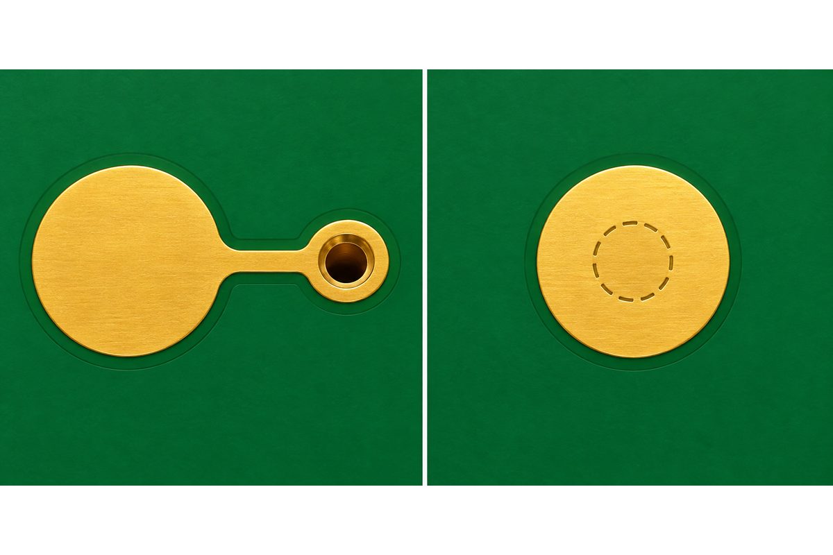
For a solderable capped land, agree on how the relevant surface and internal features will be assessed. Ask the supplier which specification applies to the cap, fill condition, and surface geometry, and which evidence is appropriate for the order. Do not copy a tolerance from an unrelated supplier or package.
Distinguish what surface inspection can show from what an internal evaluation can establish. A surface photograph can document an observable condition, but it cannot prove the complete fill or plated structure. If microsections, coupons, or other tests are required, define their scope and reporting expectations before manufacture.
When a condition is questioned, record the feature location, revision, lot, and inspection method. Compare it with the agreed acceptance requirement before selecting a cause or corrective action. A depression, apparent void, or cap concern needs product-specific evidence rather than a diagnosis based on a generic illustration.

Identify the treated vias unambiguously in the release
Provide an agreed data method that distinguishes vias needing filling and capping from other holes. That may be a separate selection layer, explicit drawing information, or another format the fabricator approves. The method should be tied to the final drill and copper data, not an old screenshot of the escape region.
Eurocircuits’ via-filling data guide illustrates why a supplier needs a clear selection of affected holes. Its order-system instructions are specific to that supplier. For your build, ask the selected fabricator which information it needs and confirm the interpretation in the engineering review.
Include the board outline, stackup, drill files, fabrication drawing, material constraints, copper requirements, surface finish, quantity, and schedule. State the via treatment and inspection requirements. If substitutions are possible, identify which changes need approval before they are incorporated into production.
Preparing a via-in-pad design for fabrication? Submit the released files, stackup, treated-via identification, quantity, and acceptance requirements through the PCB engineering and quotation request. These inputs allow the proposed construction and manufacturing scope to be reviewed before the order is finalized.
Compare alternatives with the same requirements
As a hypothetical example, a request that says only “fill the BGA vias” leaves several questions open. A better review package identifies the selected vias in matching production data, states their layer span, defines whether resin fill and a metalized cap are required, and references the agreed acceptance requirements. It also names the package and the reason a solderable land is needed. The fabricator can then confirm the proposed material, process, and evidence rather than guessing from the pad location. This example is a documentation framework, not a complete fabrication note or an approval of any particular construction.
Ask whether the routing objective can be met with a different fanout, a different layer arrangement, or a revised package choice. Compare options against the same electrical, mechanical, sourcing, and assembly requirements. A simpler fabrication route is useful only if it still supports the product design.
For a quote comparison, separate the effect of the via treatment from changes in layer count, material, drilling, inspection, and quantity. Request the assumptions behind the estimate. A lower bare-board price may not represent the same construction or the same assembly risk, so check the scope before comparing totals.
Review the design against the PCB manufacturing capabilities, and flag the proposed via-in-pad features for project-specific confirmation. General capability information does not establish that a particular fill, cap, or microvia construction has been approved.
If the treatment or layer span remains unresolved, include the alternatives and relevant package information in the fabrication quote request. Ask for an engineering review of the proposed construction, manufacturing assumptions, and inspection scope before choosing the route.
Keep fabrication and assembly revisions synchronized
A change to the package footprint, via selection, drill geometry, or stackup may require a new export and another manufacturing review. Update the affected drawing and assembly information together. A new copper file combined with an older treated-via selection can produce an inconsistent order even when each file is individually valid.
The PCB manufacturing-release checklist explains why exported data and assembly documents should describe one controlled revision. Preserve the native design and the reviewed manufacturing package so the accepted construction can be traced on repeat orders.
Use a prototype to check the intended fabrication and assembly combination. Record the component identity, board revision, process assumptions, and the relevant inspection and functional results. A passing electrical test is useful evidence for connectivity, but it does not replace other acceptance checks required by the build.
Conclusion
Via-in-pad is a routing decision that must become a clearly specified manufacturing structure. Identify the layer span and geometry, distinguish filling from capping and covering, coordinate the component land, and agree on the inspection evidence. A complete release gives the fabricator and assembler a shared basis for reviewing the design.
Ready for the next build? Submit the fabrication package, via-treatment selection, stackup, quantity, schedule, and assembly or test requirements through the online PCB RFQ form for an engineering and quotation review. Include the package documentation so the proposed pad construction can be evaluated against its actual use.
Latest Blog

Contact Info
Phone: +86-755-82882936
Email: [email protected]
WhatsApp: +86-13570802455
Wechat: +86-13570802455
Address: 2nd floor,D Bldg.,Electric Link Technology Bldg.,Gongming,Guangming New Dist.,518106 Shenzhen, China