
PCB Fiducial Marks: Layout, Panel References, and SMT Release
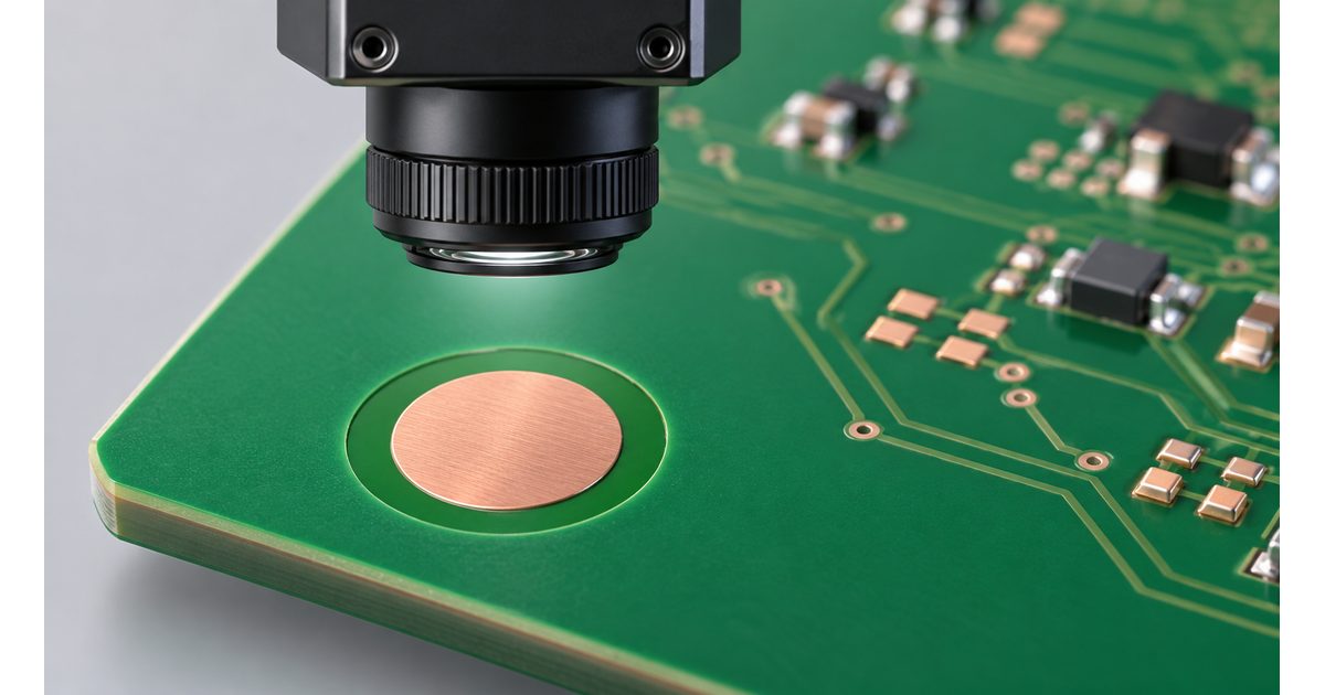
Table of Conent
Table of Conent
PCB fiducial marks give assembly equipment recognizable optical references on the board. The references help relate the physical PCB to the coordinates used for printing or component placement. A useful fiducial is a deliberately designed target that remains visible when the relevant machine needs it, not simply a convenient copper feature near a corner.
Engineers and buyers should review fiducials with the assembly process, panel arrangement, and released data. This guide explains how to distinguish their roles, avoid obscured or ambiguous targets, and prepare an SMT package that the assembler can interpret consistently. Equipment-specific requirements still need confirmation for the actual build.
Define which operation will use the reference
Identify whether the target supports solder-paste printing, component placement, or another approved vision operation. These processes may use related references, but their visibility and programming requirements are not necessarily identical. A target available on a bare board may become obscured later in the assembly sequence.
Eurocircuits’ fiducial guidelines describe the use of copper targets by printers and placement machines, including panel and individual-board references. Its stated requirements belong to its manufacturing arrangement. Use that example to frame the review, not to assume that every assembly line needs the same target count or placement.
Ask the assembler which board faces and stages require targets. For double-sided assembly, review each face independently. A reference on the opposite side is not automatically available to the camera or suitable for the program being created.
Distinguish panel, board, and component-local references
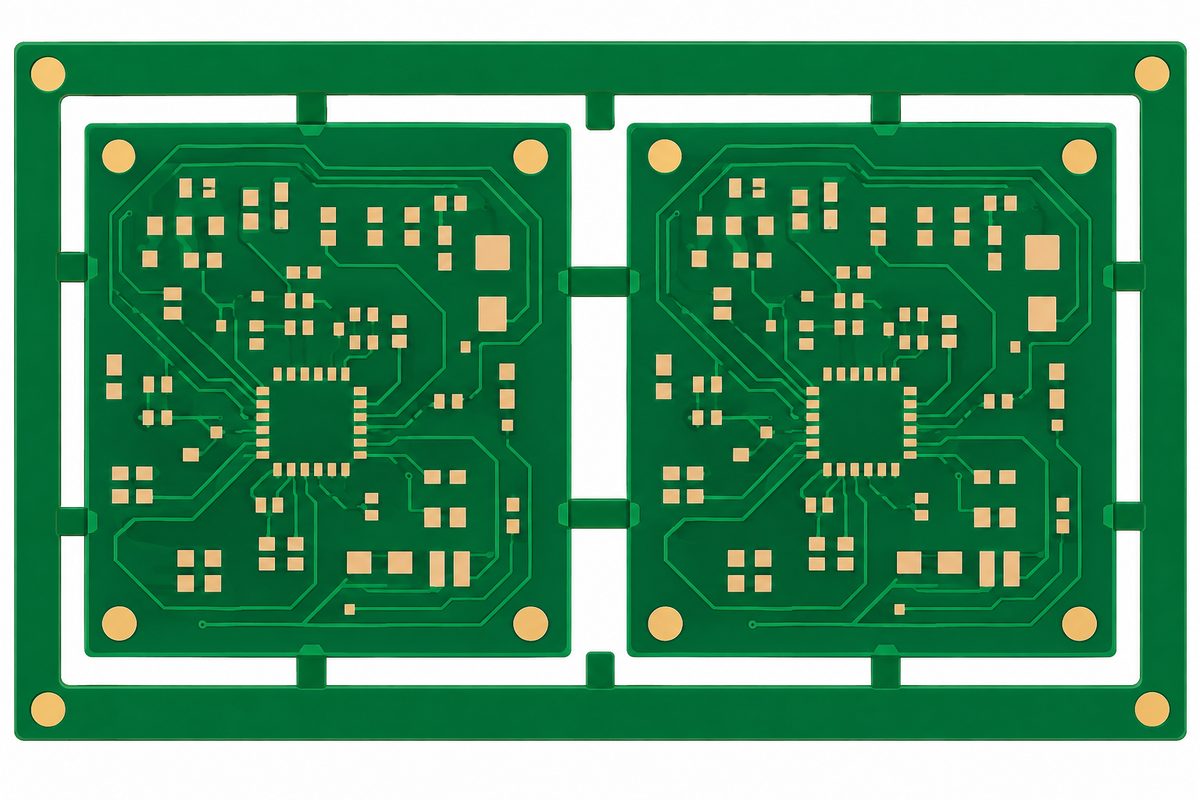
A panel reference locates the assembly panel as presented to the equipment. A board-level reference identifies an individual circuit within that arrangement. A component-local reference, where required, supports registration near a particular placement area. Define these roles explicitly because suppliers may use the words “global” and “local” differently.
Panel targets do not automatically eliminate a need for individual-board references. Conversely, adding many targets near components without a process requirement can consume layout space without improving the operation. Agree on the selected references and the problem each one is intended to address.
The PCB panelization guide explains the broader rail and separation arrangement. For fiducials, the panel review should identify who adds the rail targets and how the machine will distinguish the relevant individual-board locations.
Use a recognizable copper target rather than a hole
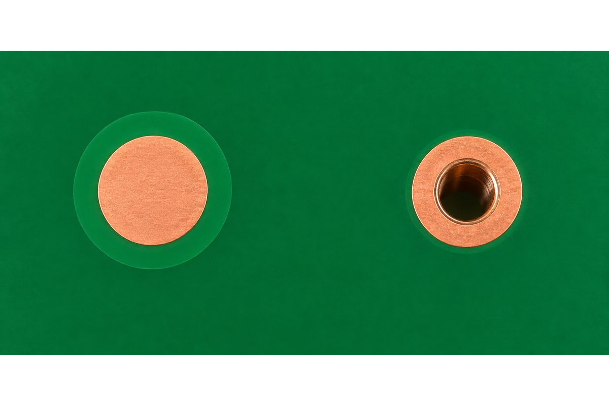
Define the target shape, size, surface condition, and surrounding clearance according to the agreed assembly requirements. A solid circular copper target is a common design form. Do not confuse it with a via, mounting hole, or annular ring that has a different geometry and manufacturing purpose.
Keep the fiducial distinct from silkscreen orientation marks. Printed text or an arrow can help a person identify a board, but it does not replace the copper target specified for a machine’s registration method. Also avoid assuming that a nearby component pad will be accepted as an equivalent reference.
Do not add a paste deposit over the optical target as though it were a solderable component land. Review the copper, solder-mask, and paste layers together so the exported files preserve the intended surface. The appropriate finish and mask opening must be agreed with the supplier rather than inferred from the target’s appearance in CAD.
Reserve clear space around the target
A camera needs an identifiable target and a usable surrounding area. Review nearby copper, silkscreen, solder-mask features, component bodies, and other objects against the assembler’s recognition requirements. A correct target shape can still be difficult to use if the surrounding pattern is confusing.
Check the target in the condition in which it will be recognized. Components placed earlier, a fixture, a clamp, or a panel support feature can obstruct a location that looked accessible in the layout editor. Discuss the actual transport and support arrangement before accepting a target close to the edge.
Keep target geometry consistent within the agreed set where the process requires it. Mixing shapes or unintended mask openings can complicate recognition and setup. Resolve differences in the released design rather than expecting the programmer to reinterpret each target individually.
Place references with orientation and process access in mind
Discuss the distribution of the selected targets across the relevant panel or board. The machine’s alignment method determines the useful arrangement. Avoid treating a small cluster of convenient marks as equivalent to a reviewed set that supports the intended registration task.
Make the board’s orientation unambiguous in the manufacturing data and assembly instructions. Where the supplier requests an asymmetric reference arrangement, implement that requirement consistently rather than changing it during panel preparation. A target pattern and a separate orientation note should describe the same physical setup.
Review local references around fine-pitch or other demanding placements with the assembler. The need depends on the equipment, board behavior, and placement requirement. Neither a component package name nor a nominal pitch alone proves that a particular target arrangement is sufficient.
Preparing an SMT prototype? Send the PCB files, panel proposal, placement data, BOM, target locations, and quantity through the SMT engineering and quotation request. Ask for a review of reference visibility, clearance, and the proposed registration approach before the order scope is finalized.
Keep coordinates and reference definitions synchronized
The machine program must identify the physical targets corresponding to the released data. Eurocircuits’ pick-and-place setup explanation includes defining fiducials in the program to align with the board. The practical handoff is to name and locate the intended references clearly instead of relying on visual recognition of an old prototype.
Confirm the coordinate origin, units, board face, and rotation convention for the placement data. For a panelized build, clarify whether coordinates describe a single board or the complete panel. Do not combine a panel-level reference drawing with an unexplained single-board coordinate file.
The PCB manufacturing-release checklist explains why exports and assembly documentation need a consistent revision. Fiducial copper, mask openings, placement coordinates, and panel references belong in the same controlled release.
Separate design ownership from panel preparation
State whether the PCB designer or manufacturer supplies the panel-rail targets. If the supplier adds them, ask for the proposed arrangement and any impact on rail dimensions or support. Do not assume that an automatic panelization step resolves every reference needed on an individual board.
Record any approved changes to the board or panel. A manufacturer-added target should not cover unrelated copper, replace a functional feature, or conflict with a required edge condition. Keep the approval accessible to the team creating the assembly program.
Review the proposed manufacturing package against the SMT assembly service and request project-specific confirmation of the reference arrangement. A general service description does not establish that a specific camera, fixture, and target design have been qualified together.
Check exported artwork and the first setup
Preview the final copper, mask, paste, and legend data. Verify that the selected targets remain present on the correct face, retain the agreed clear area, and are not assigned unintended paste openings. A library symbol that looked correct earlier can still export differently after layer or footprint edits.
During initial setup, confirm that the intended physical targets are recognized and that the resulting registration is consistent with the board orientation and program. Review the relevant setup evidence and placement or printing results before treating target recognition as proof of the finished assembly quality.
If recognition is unreliable, preserve the actual observation before changing the design or camera setup. Check obstruction, target condition, surrounding features, data identity, and orientation as appropriate. Do not attribute every placement error to fiducials without reviewing the other parts of the process.

Include fiducials in the RFQ and change-control review
Provide the released board revision, BOM, assembly drawing, placement data, panel details, and any assembler-confirmed fiducial requirements. Identify which decisions are still open and who must approve them. This avoids a quotation based on references that later disappear from the manufactured panel.
Where the arrangement remains uncertain, attach the current files and list the target, face, or panel questions in the PCB assembly quotation request. Ask for engineering review so the quote can distinguish the agreed release from remaining preparation work.
As a hypothetical example, adding an underside component near a previously approved target may obscure it during a later operation. The electrical design can remain unchanged while the registration plan becomes unusable. Recheck visibility after component, panel, support, or assembly-sequence changes.
Conclusion
PCB fiducial marks work as part of a defined registration process. Select the reference roles, preserve recognizable copper targets and clear surroundings, coordinate both board faces, and release consistent panel and placement data. Validate the actual setup rather than assuming that the presence of copper dots guarantees assembly accuracy.
Ready for the next build? Submit the released PCB files, BOM, placement data, panel drawing, quantity, schedule, and assembly requirements through the online PCB RFQ form for engineering and quotation review. Highlight the intended fiducials and open registration questions so they can be checked before production.
Latest Blog
Contact Info
Phone: +86-755-82882936
Email: [email protected]
WhatsApp: +86-13570802455
Wechat: +86-13570802455
Address: 2nd floor,D Bldg.,Electric Link Technology Bldg.,Gongming,Guangming New Dist.,518106 Shenzhen, China