
Arduino Nano Carrier PCB Design: Pinout, Power, and DFM
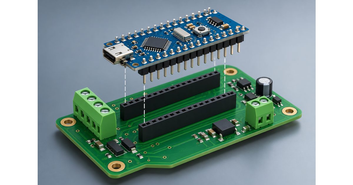
Table of Conent
Table of Conent
An Arduino Nano can help validate a circuit on a breadboard, but moving that circuit to a custom carrier PCB introduces new decisions. The module orientation, power architecture, connector positions, programming access, and manufacturing package all need to agree. A prototype that worked with loose wires does not automatically become a repeatable assembled product.
This guide focuses on integrating the classic Nano into a carrier board and preparing that carrier for fabrication. It explains how to use the official pinout, review electrical interfaces, and document a build. It also identifies the questions to revisit when changing to another Nano-family board or a third-party module.
Identify the exact Nano before drawing the carrier
Arduino’s classic Nano hardware page identifies a breadboard-oriented module with headers, a Mini-B USB connector, and a nominal 45 mm by 18 mm board outline. Use the linked CAD files and mechanical information for the footprint instead of turning those overall dimensions into an assumed header pattern.
The classic Nano is one member of a broader family. A similar outline or name does not establish identical electrical behavior, power connections, or software configuration. Record the exact module part number and revision in your design documents. For a third-party board, obtain its own schematic and mechanical drawing rather than assuming every detail matches Arduino’s original.
If the carrier needs to accept several variants, create an explicit compatibility list. Check each variant against the carrier’s power, signal, programming, and mechanical requirements. An unverified substitution should not be treated as a purchasing shortcut simply because the board appears to fit the sockets.
Use the official pinout as a controlled input
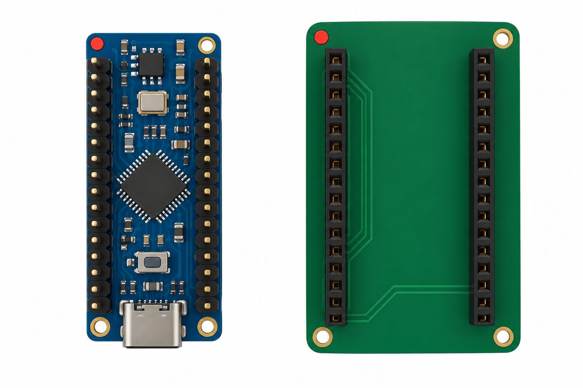
For the classic Nano, the official A000005 pinout identifies A4 as SDA and A5 as SCL, with D0/RX and D1/TX serving the serial interface. These mappings belong to the named module. Preserve the drawing’s orientation when translating the header connections into a carrier symbol and footprint.
Create a connection table for your project: module pin name, carrier net name, destination, signal direction, and voltage expectation. Then compare that table with the schematic and the actual module. This is more reliable than copying an unlabelled footprint and assigning nets from memory.
Check which view each drawing uses. Looking at the bottom of a module can reverse the apparent header order. Mark the installation orientation clearly on the carrier and assembly drawing, and verify it with a physical sample before ordering a production quantity.
Review the power paths before connecting peripherals
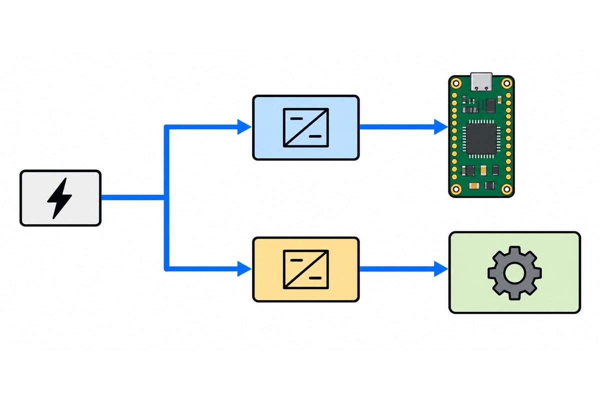
The classic Nano user manual describes USB and VIN power paths, a regulated 5 V supply connection, and 5 V serial signaling. Review the exact board documentation when selecting the supply and interfaces. Do not transfer the classic board’s assumptions to a different Nano variant.
Define where the carrier receives power and how that power reaches the module and external loads. Consider what happens when USB is connected while the external supply is present. Confirm the intended power-path behavior against the module schematic; do not assume two sources can be connected together without review.
Budget peripheral current separately from logic signaling. Motors, relays, and other substantial loads need appropriate power and driver circuitry rather than being treated as direct GPIO loads. For every external device, check its input thresholds, supply range, and interface requirements against the selected module.
Give the schematic clear rail names and identify the required return paths. If a sensor or peripheral uses a different logic level, assess whether a compatible interface or level translation is needed. The carrier design should make that decision explicit instead of leaving it to the person who assembles the prototype.
Plan the carrier layout around real interfaces
Place the module, external connectors, mounting holes, and enclosure boundaries before detailed routing. Confirm that the USB cable can be inserted after the carrier is mounted. Review the module’s underside clearance and the assembled height, including sockets and the components beneath or around it.
Choose socketed or soldered installation deliberately. Sockets can simplify module replacement and early debugging, while a soldered installation changes servicing and assembly assumptions. Record the selected header and socket parts, their orientation, and any assembly instructions needed to achieve the intended height.
A straightforward carrier may be suitable for a two-layer construction, but the decision depends on routing, grounding, power distribution, and the product requirements. The two-layer PCB stackup and design guide helps frame those tradeoffs. Avoid selecting the layer count solely because the breadboard prototype used few connections.
Preserve programming and debugging access
Test the software workflow with the exact module before locking the enclosure and carrier geometry. Confirm the intended development environment, board configuration, port, and upload procedure. Include a simple known-good program in the prototype plan so hardware and software problems can be separated during bring-up.
Review peripherals connected to serial or programming-related signals. An attached device can affect communication or startup if its behavior conflicts with the module’s programming path. Decide whether the prototype needs an isolation option, accessible connector, or another documented provision for troubleshooting.
For assembled builds, define which firmware image is required, how it is identified, and what happens after programming. An upload that finishes successfully is different from a functional test of the completed carrier. Specify the checks that demonstrate the relevant inputs, outputs, and interfaces work as intended.
Use a prototype to answer concrete questions
Ask the assembler how the two socket rows will be kept aligned and how the module fit will be checked. Correct electrical connections do not prove that a module can be inserted without loading the solder joints or bending the headers. Define the mechanical fit expectation and whether installation is included in the build. If the module will be soldered directly, confirm the proposed soldering process and handling requirements with its supplier before approving the assembly route. These details belong in the release instructions, not only in the prototype team’s memory.
Choose an example project that exercises the carrier’s important interfaces. A sensor interface can test signal compatibility and connector mapping; a small data-acquisition prototype can test power and measurement access; a control-interface prototype can test output-driver behavior. These are example validation directions, not claims that a generic carrier is qualified for every application.
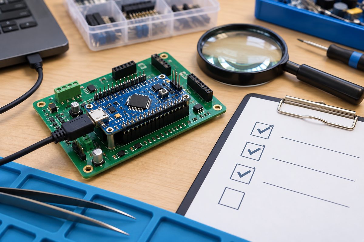
For the first assembly, plan an orderly bring-up sequence. Inspect orientation and soldering, check the relevant power nets before normal operation, then validate programming and the intended functions. Use suitable instruments and procedures for the circuit. Record observations against the carrier and module revisions rather than relying on an informal demonstration.
Prepare the fabrication and assembly release
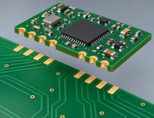
Release the carrier’s Gerber and drill files with a fabrication drawing, board thickness, material requirements, surface finish, quantity, and schedule. State the mechanical constraints that matter to socket fit or enclosure mounting. A rendering of the module on a board is useful context, but it cannot replace the manufacturing data.
For assembly, provide the BOM, placement data, assembly drawing, module identity, and installation instructions. Identify whether modules and connectors are customer-supplied or part of the sourcing request. Include any firmware, programming procedure, and test expectations required for the completed assembly.
The PCB design and manufacturing-release checklist explains why exported files and assembly data need a consistent revision. Apply the same discipline to the carrier even when the controller module is bought as a finished item.
Ready for a carrier prototype? Send the fabrication files, module drawing, BOM when assembly is required, quantity, and test expectations through the PCB engineering and quotation request. The package allows the manufacturing and assembly scope to be reviewed against the actual design.
Compare sourcing and build options clearly
Review the carrier requirements against the PCB manufacturing capabilities. Identify unusual mechanical features, special inspection needs, or installation operations before seeking a combined quote. Supplier capability information is a starting point; the carrier and assembly still need their own review.
Separate the cost and responsibility for the bare carrier, module procurement, component sourcing, soldering, programming, and test work. For repeat orders, document which substitutions need approval. Changing the module can affect more than the BOM: it may require another power, compatibility, firmware, and fit review.
For a combined build, include those scope decisions in the carrier fabrication and assembly quote request. Provide the released files and sourcing preferences so the engineering team can clarify open requirements and prepare a relevant quotation.
Conclusion
An Arduino Nano carrier is most useful when the module and custom PCB are treated as one controlled assembly. Verify the exact pinout and orientation, review power and signal compatibility, preserve programming access, and define prototype acceptance checks. Then release the documents that allow the build to be repeated.
Starting the next prototype? Submit the carrier files, module part number, assembly data, quantity, schedule, and test requirements through the online PCB RFQ form for an engineering and quotation review. Include the module documentation so the review can address the specific integration.
Latest Blog
Contact Info
Phone: +86-755-82882936
Email: [email protected]
WhatsApp: +86-13570802455
Wechat: +86-13570802455
Address: 2nd floor,D Bldg.,Electric Link Technology Bldg.,Gongming,Guangming New Dist.,518106 Shenzhen, China