
2-Layer PCB: Stackup, Design Rules, Cost & Manufacturing
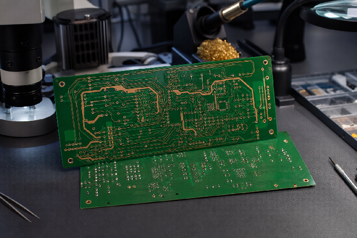
Table of Conent
Table of Conent
A 2-layer PCB is a printed circuit board with copper on both sides of the substrate. It is the most common upgrade from a single-sided board when your layout needs cleaner routing, better grounding, smaller size, or fewer jumpers without moving into the cost and complexity of a full multilayer PCB.
If you have ever tried to route a power supply, microcontroller board, sensor module, or connector-heavy design on one copper layer, you know the moment when the layout starts fighting back. Traces take long detours. Jumpers appear. Ground returns become messy. That is usually where a two-layer board earns its keep.
This guide explains how 2-layer PCBs are built, when they make sense, how to choose a stackup, which design rules matter, and what to check before sending files to fabrication.
Key Takeaways
– A 2-layer PCB gives you copper on the top and bottom sides, making routing easier than a 1-layer board while staying cheaper than most multilayer designs.
– The biggest design advantage is not just extra routing space. It is the ability to create cleaner ground returns, shorter traces, and more flexible component placement.
– Good via strategy, copper balance, trace width, spacing, and panelization all affect yield and cost.
– A 2-layer board is not ideal for dense BGA packages, high-speed buses, RF layouts, or complex power distribution. Those usually need a multilayer stackup.
– The safest design release includes Gerbers, drill files, board thickness, copper weight, surface finish, impedance needs if any, and clear assembly notes.
What Is a 2-Layer PCB?
A 2-layer PCB, also called a double-sided PCB or two-layer PCB, has one copper layer on the top side and one copper layer on the bottom side. The two copper layers are separated by an insulating core, usually FR-4 for standard rigid boards.
The two layers connect through plated through holes, usually called vias. Those vias let a signal, power trace, or ground connection move from one side of the board to the other.
The basic structure looks like this:
| Layer / Feature | Typical Material | Purpose |
|---|---|---|
| Top solder mask | Epoxy-based solder mask | Protects copper and defines solderable pads |
| Top copper | 0.5 oz, 1 oz, or 2 oz copper | Carries signals, power, pads, and copper pours |
| Core dielectric | FR-4 or other laminate | Provides insulation and mechanical strength |
| Bottom copper | 0.5 oz, 1 oz, or 2 oz copper | Carries routing, ground areas, and return paths |
| Bottom solder mask | Epoxy-based solder mask | Protects copper and improves soldering control |
| Surface finish | HASL, ENIG, OSP, immersion tin/silver | Preserves exposed pads for soldering |
Compared with a 1-layer PCB, the second copper layer gives the designer more freedom. You can route traces on one side and use the other side for return paths or crossovers. You can also reduce wire jumpers and keep the board outline smaller.
Compared with a multilayer PCB, a 2-layer board is simpler and cheaper to fabricate. There are no internal layers, no lamination cycle for multiple cores and prepregs, and fewer stackup variables to manage.
When a 2-Layer PCB Is the Right Choice
A 2-layer PCB is often the practical middle ground between “simple and cheap” and “dense and controlled.” It works best when the circuit is not too dense, but still needs routing flexibility beyond a single copper side.
Typical applications include:
- microcontroller development boards
- LED control boards
- power supply modules
- sensor boards
- relay and interface boards
- consumer electronics boards
- small industrial control boards
- IoT gateway and peripheral boards
- simple automotive auxiliary modules
The strongest reason to choose a two-layer board is usually layout quality. You get shorter routes, fewer crossovers, and better component placement. You can place connectors where the product needs them instead of where the routing forces them.
Here is a practical decision table:
| Design Situation | 1-Layer PCB | 2-Layer PCB | Multilayer PCB |
|---|---|---|---|
| Simple LED or relay board | Good fit | Good if routing is tighter | Usually unnecessary |
| Microcontroller with connectors | Often crowded | Good fit | Needed only for density or EMC |
| Dense fine-pitch ICs | Poor fit | Limited | Better fit |
| Controlled impedance routing | Poor fit | Possible but limited | Usually best |
| High-speed memory or RF | Poor fit | Risky | Usually required |
| Lowest bare-board cost | Best | Moderate | Higher |
| Clean ground return | Limited | Better | Best |
In practice, many products start as 2-layer prototypes because they give engineers enough routing freedom without making the first build expensive.
How a 2-Layer PCB Stackup Works
The word “stackup” sounds more complicated than it is for a two-layer board. In most standard designs, the stackup is simply top copper, FR-4 core, and bottom copper.
The important choices are board thickness, copper weight, and how you assign routing and copper pours on each side.
Common 2-Layer PCB Stackups
| Finished Thickness | Copper Weight | Common Use | Notes |
|---|---|---|---|
| 0.8 mm | 1 oz | compact electronics, small modules | More flexible, check connector stress |
| 1.0 mm | 1 oz | handheld products, compact boards | Good balance of size and rigidity |
| 1.2 mm | 1 oz | medium-size control boards | Less common than 1.6 mm but still practical |
| 1.6 mm | 1 oz | default general-purpose PCB | Broadly available, mechanically stable |
| 1.6 mm | 2 oz | higher-current or thermal designs | Wider process margin needed for etching |
| 2.0 mm+ | 1 oz or 2 oz | heavy connectors or mechanical load | Higher cost, check enclosure fit |
For most general electronics, 1.6 mm finished thickness with 1 oz copper is the default. It is widely available, mechanically stable, and cost-effective.
But “default” does not mean “always correct.” A compact IoT board may need 1.0 mm thickness to fit the enclosure. A power board may need 2 oz copper for current and heat. A board with heavy terminal blocks may need extra thickness for mechanical support.
Top and Bottom Layer Assignment
There is no universal layer assignment that works for every two-layer board, but a common pattern is:
- top layer for components and primary signal routing
- bottom layer for ground pour, return paths, and secondary routing
That does not mean the bottom layer should be a perfect ground plane. On a 2-layer PCB, it often cannot be. Vias, routing channels, connectors, and power traces will break it up. Still, keeping one side as continuous as possible helps signal integrity and EMI behavior.
Texas Instruments has long emphasized in board layout guidance that current return paths and loop area matter for noise-sensitive designs. You do not need an advanced high-speed board to benefit from that principle. Even a modest microcontroller board works better when signals have short, clean returns.
2-Layer PCB Design Rules That Matter
A two-layer board gives you more room than a one-layer board, but it does not remove the need for design discipline. The common failures are usually simple: thin traces for current, too few vias, poor ground continuity, and tight clearances that were not necessary.
Trace Width and Current
Trace width depends on copper weight, current, acceptable temperature rise, and routing space. The numbers below are not a substitute for final engineering calculation, but they are useful for early design planning.
| Current Level | Typical Starting Point on 1 oz Copper | Design Note |
|---|---|---|
| Signal traces | 6-10 mil | Check fabricator capability and assembly class |
| 100-300 mA | 10-20 mil | Common for small logic and sensor power |
| 500 mA-1 A | 25-50 mil | Keep traces short where possible |
| 1-2 A | 60-100+ mil | Consider copper pours or 2 oz copper |
| Above 2 A | Calculate carefully | Use copper pours, thermal vias, or heavier copper |
Many low-cost problems start when a designer routes power like a signal. A trace that works electrically in CAD may still run warm, drop voltage, or become fragile during rework.
If current is a major driver in your board, this article on why copper is used in circuit board manufacturing gives useful background on copper thickness, conductivity, and fabrication trade-offs.
Via Strategy
Vias are the main advantage of a 2-layer board. They are also easy to overuse.
Use vias to:
- escape crowded routing areas
- connect top and bottom ground pours
- shorten signal paths
- provide thermal connection to copper areas
- reduce loop area for return currents
Avoid placing vias where they create assembly or reliability problems. For example, vias too close to small SMT pads can pull solder away during reflow. Vias inside pads need special processing if they are not tented, plugged, or filled.
For most standard two-layer boards, ordinary through vias are enough. Keep the via dimensions within the fabricator’s standard process when possible. There is no benefit in specifying tiny vias if the board does not need them.
Grounding on a 2-Layer PCB
Grounding is where two-layer boards get interesting. You have only two copper layers, so a perfect reference plane is difficult. Still, you can improve the layout significantly by planning ground early.
Good practices include:
- use a ground pour on both layers where possible
- stitch ground areas with vias
- avoid cutting return paths under sensitive signals
- keep high-current return paths away from sensitive analog sections
- place decoupling capacitors close to IC power pins
- keep oscillator and clock loops short
The goal is not a textbook-perfect plane. The goal is a low-impedance return structure that does not force current to wander across the board.
Component Placement
Routing problems often start before the first trace is drawn.
On a 2-layer PCB, placement should consider:
- connector position
- power entry point
- current flow
- signal grouping
- mechanical mounting holes
- assembly access
- test point access
If the placement is poor, the second copper layer will not rescue the design. It will only make the routing look finished while the current paths remain messy.
Manufacturing Choices That Affect Cost
Two-layer boards are affordable because they use a mature, standard fabrication flow. Cost still moves quickly when the design asks for tighter process control, heavier copper, special materials, unusual finishes, or complex mechanical features.
Main Cost Drivers
| Cost Driver | Low-Cost Choice | Higher-Cost Trigger |
|---|---|---|
| Material | Standard FR-4 | High-Tg, halogen-free, metal-core, RF laminate |
| Thickness | 1.6 mm | Very thin, very thick, or non-standard thickness |
| Copper weight | 1 oz | 2 oz or heavier |
| Trace/space | Standard rules | Fine lines and tight spacing |
| Hole size | Standard mechanical drills | Small drills, slots, or tight tolerance |
| Surface finish | HASL or OSP | ENIG, immersion silver, hard gold |
| Outline | Simple routed shape | Complex routing, slots, castellations |
| Testing | Standard electrical test | Extra inspection or documentation |
The best way to reduce cost is not always to choose cheaper materials. It is often to avoid unnecessary process difficulty.
For example, changing a via from a non-standard small drill to a standard drill may reduce cost without affecting performance. Increasing clearance near the board edge may improve yield with no electrical penalty. Choosing HASL instead of ENIG may be fine for through-hole-heavy boards.
That is the kind of feedback a good DFM review should provide.
Surface Finish Selection
Surface finish affects solderability, shelf life, pad flatness, and price.
| Surface Finish | Best Fit | Advantage | Trade-Off |
|---|---|---|---|
| Lead-free HASL | General-purpose boards, larger SMT, through-hole | Low cost and widely available | Less flat than ENIG |
| ENIG | Fine-pitch SMT, test pads, longer storage | Flat, stable surface | Higher cost |
| OSP | Cost-sensitive production with quick assembly | Low cost, flat copper surface | Shorter shelf and handling window |
| Immersion tin | Press-fit or selected soldering needs | Good solderability | Handling sensitivity |
| Immersion silver | Some signal and solderability applications | Good conductivity and flatness | Tarnish control required |
If the board uses fine-pitch components, ENIG may be worth the cost. If the board is mostly through-hole connectors and large pads, lead-free HASL may be enough.
2-Layer PCB vs 1-Layer PCB vs Multilayer PCB
The layer count decision should come from the circuit, not from habit.
| Factor | 1-Layer PCB | 2-Layer PCB | Multilayer PCB |
|---|---|---|---|
| Routing flexibility | Low | Moderate | High |
| Bare-board cost | Lowest | Low to moderate | Higher |
| Board size | Often larger | Usually smaller | Smallest for dense designs |
| Ground quality | Limited | Better | Best |
| EMI control | Limited | Moderate | Stronger |
| Assembly efficiency | Good for simple boards | Good for mixed designs | Good for dense designs |
| Best use case | Simple, low-cost circuits | General electronics and prototypes | Dense, high-speed, RF, complex power |
The key point is that a 2-layer PCB is not automatically better than a 1-layer board. If the circuit is simple and cost is the only major driver, a single-sided board may still be the right answer.
But once the one-layer version needs multiple jumpers, awkward routing, or a larger outline, the two-layer option often becomes cheaper at the product level.
Common DFM Issues on 2-Layer Boards
Most two-layer DFM issues are avoidable. They usually come from pushing the board into unnecessary tight tolerances or leaving manufacturing details undefined.
Issues We See Often
| Issue | Why It Matters | Practical Fix |
|---|---|---|
| Thin annular rings | Drill tolerance can break the pad | Increase pad size or use standard drill sizes |
| Copper too close to edge | Routing can expose copper | Pull copper back from routed outline |
| Poor ground stitching | Return paths become noisy | Add stitching vias near layer transitions |
| Overly narrow power traces | Voltage drop and heating increase | Widen traces or use copper pours |
| Vias near SMT pads | Solder can wick into vias | Move vias away or tent them |
| Unbalanced copper | Board can warp or etch unevenly | Balance pours where practical |
| Missing panel rails | Assembly handling becomes harder | Add rails and fiducials for PCBA |
A good manufacturer should catch many of these during file review. Better still, the layout should avoid them before release.
If the board will go into assembly, panel planning matters early. This guide to PCB panelization explains why panel layout can affect yield, handling, and total cost.
What to Send Your Manufacturer
The fastest way to slow down a simple PCB order is to send incomplete manufacturing data.
For a 2-layer PCB quote or build, send:
- Gerber files
- NC drill file
- board outline
- finished board thickness
- copper weight
- solder mask color
- surface finish
- quantity
- target lead time
- impedance requirements if any
- assembly notes if PCBA will follow
If assembly is involved, also send:
- BOM
- pick-and-place file
- assembly drawing
- polarity notes
- test requirements
For early validation builds, a PCB prototype run with DFM feedback is usually the safest path. The goal is not just to receive boards quickly. The goal is to catch problems before the design becomes expensive to change.
A Practical 2-Layer PCB Design Checklist
Use this checklist before releasing files:
| Check | What to Confirm |
|---|---|
| Stackup | Thickness, copper weight, and material are defined |
| Trace width | Power traces are sized for current and temperature rise |
| Spacing | Clearances meet manufacturer rules and voltage needs |
| Vias | Via size is standard unless smaller vias are necessary |
| Ground | Ground pours are stitched and return paths are not cut unnecessarily |
| Decoupling | Capacitors are close to IC power pins |
| Edge clearance | Copper is pulled back from board outline |
| Finish | Surface finish matches component pitch and shelf-life needs |
| Panelization | Rails, fiducials, and breakaway method are considered |
| Files | Gerbers, drill files, and outline are complete |
This is not a substitute for a full DFM review, but it catches many common mistakes before files leave your desk.
Final Thoughts
A 2-layer PCB is often the most practical board type for prototypes, control circuits, sensor modules, power interfaces, and general electronics. It gives you enough routing freedom to avoid the worst limits of single-sided boards while keeping fabrication cost far below most multilayer designs.
The best results come from treating the second layer as an engineering tool, not just extra routing space. Use it to shorten traces, improve ground returns, reduce jumpers, simplify placement, and make the board easier to assemble.
Before ordering, define the stackup, copper weight, surface finish, and testing expectations clearly. Then ask your manufacturer to review the files for drill margin, edge clearance, via placement, copper balance, and panelization. Those checks are simple, but they prevent expensive surprises.
Need a second set of manufacturing eyes on your 2-layer PCB? Send your Gerbers, drill files, BOM if available, and target quantity. A good DFM review should tell you what is ready, what is risky, and what can be simplified before fabrication starts.
Request a free DFM-backed PCB quote.
Frequently Asked Questions About 2-Layer PCB
What is the difference between a 2-layer PCB and a double-sided PCB?
There is no practical difference. A 2-layer PCB and a double-sided PCB both have copper on the top and bottom sides of the board, with plated holes or vias connecting the two layers.
Is a 2-layer PCB cheaper than a 4-layer PCB?
Yes, a 2-layer PCB is usually cheaper than a 4-layer PCB because it has fewer copper layers and a simpler fabrication process. A 4-layer board can still be the better choice for dense routing, cleaner power distribution, or high-speed performance.
Can a 2-layer PCB have a ground plane?
It can have ground pours, but it usually does not have a perfect uninterrupted ground plane. Routing, vias, connectors, and power traces often break up the copper. Good via stitching and careful routing help maintain better return paths.
What is the standard thickness for a 2-layer PCB?
The most common finished thickness is 1.6 mm, usually with 1 oz copper. Other thicknesses such as 0.8 mm, 1.0 mm, 1.2 mm, and 2.0 mm are also common depending on enclosure, mechanical, and current requirements.
When should I move from a 2-layer PCB to a multilayer PCB?
Move to a multilayer PCB when routing becomes too dense, ground return paths are poor, controlled impedance is required, EMI risk is high, or the design includes high-speed buses, RF sections, or fine-pitch BGAs.
Latest Blog

Contact Info
Phone: +86-755-82882936
Email: [email protected]
WhatsApp: +86-13570802455
Wechat: +86-13570802455
Address: 2nd floor,D Bldg.,Electric Link Technology Bldg.,Gongming,Guangming New Dist.,518106 Shenzhen, China