
2-Layer PCB Manufacturer: How to Choose the Right One
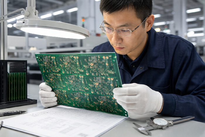
Table of Conent
Table of Conent
A good 2-layer PCB manufacturer should do more than produce a cheap double-sided board. The right supplier should help you confirm stackup, copper weight, drill rules, surface finish, panelization, testing, and assembly readiness before the first panel goes into production.
That sounds like a lot for a common board type. But 2-layer boards sit in a tricky middle ground. They are simple enough that buyers often treat them like a commodity, yet important enough to carry microcontrollers, power rails, connectors, sensors, and production-critical interfaces. A weak supplier can still create expensive problems: noisy ground returns, poor via plating, bad panel rails, unstable solderability, or late assembly changes.
This guide explains how to evaluate a 2-layer PCB manufacturer from an engineering and sourcing perspective. The goal is simple: choose the supplier that gives you the lowest project risk, not just the lowest line-item price.
Key Takeaways
– A reliable 2-layer PCB manufacturer should confirm stackup, copper weight, drill capability, finish, and testing before production.
– The most valuable supplier feedback usually appears during DFM review, especially around vias, edge clearance, ground pours, and panelization.
– For prototypes, fast response and practical engineering comments often matter more than a small price difference.
– For production, repeatability, traceability, panel quality, and assembly support become more important than headline turnaround time.
– If the board will move into PCBA, choosing a manufacturer with fabrication and assembly under one workflow usually reduces revision loops.
What a 2-Layer PCB Manufacturer Actually Controls
A 2-layer PCB manufacturer fabricates printed circuit boards with copper on both sides of the substrate. The two copper layers are connected by plated through holes and vias. That basic process is mature, but the details still matter.
The manufacturer controls much more than the board outline:
| Manufacturing Area | What the Supplier Controls | Why It Matters |
|---|---|---|
| Stackup | Core material, board thickness, copper weight | Affects rigidity, routing, cost, and reliability |
| Drilling | Hole size, positional tolerance, plating quality | Critical for vias, connectors, and through-hole parts |
| Imaging and etching | Trace width, spacing, copper balance | Affects yield and electrical performance |
| Solder mask | Registration, dam width, mask clearance | Reduces solder bridging and assembly defects |
| Surface finish | HASL, ENIG, OSP, immersion tin/silver | Controls solderability, flatness, and shelf life |
| Panelization | Rails, tabs, V-score, fiducials | Affects assembly handling and cost |
| Testing | Electrical test, inspection, traceability | Reduces escape defects before shipment |
If a supplier cannot explain these areas clearly, the low quote may not mean much. You need process confidence, not just capacity.
For the board-level basics, this guide on 2-layer PCB stackup, design rules, and manufacturing is a useful reference before comparing suppliers.
When a 2-Layer PCB Manufacturer Is the Right Fit
Most electronics teams use 2-layer boards when they need more routing flexibility than a single-sided board but do not need the cost or density of a multilayer design.
Common fits include:
- microcontroller boards
- power interface boards
- LED and lighting controllers
- sensor boards
- relay and I/O modules
- simple automotive auxiliary boards
- industrial control boards
- consumer electronics boards
- prototype validation boards
The important question is not whether the manufacturer can build a 2-layer board. Almost any PCB shop can say yes. The better question is whether the supplier understands your board’s real constraints.
For example, a low-speed relay board and a compact microcontroller board may both be 2-layer designs. They do not need the same review. The relay board may care more about creepage, copper width, connector stress, and panel breakaway. The microcontroller board may care more about ground return, decoupling, via placement, and test access.
That difference should show up in the supplier’s DFM comments.
Supplier Evaluation: The 7 Checks That Matter
When comparing 2-layer PCB manufacturers, we usually start with seven checks. These are simple enough for sourcing teams to use, but technical enough to reveal whether the supplier is paying attention.
1. Stackup Confirmation
For a standard 2-layer board, the stackup may look obvious: top copper, FR-4 core, bottom copper. Still, the supplier should confirm the details.
| Stackup Item | Typical Starting Point | Questions to Ask |
|---|---|---|
| Finished thickness | 1.6 mm | Does the enclosure or connector need another thickness? |
| Copper weight | 1 oz | Does current, heat, or pad strength require 2 oz? |
| Material | Standard FR-4 | Is high-Tg, halogen-free, or special material needed? |
| Solder mask | Green | Does AOI, branding, or LED reflection need another color? |
| Finish | HASL or ENIG | Does the component pitch require a flatter finish? |
The best suppliers do not make these choices silently. They confirm them so the quote and the finished board match the same assumptions.
2. Drill and Via Capability
Vias are what make a 2-layer board useful. Poor via planning is also one of the fastest ways to create yield or reliability problems.
Ask the manufacturer:
- What is your standard minimum mechanical drill?
- What finished hole tolerance applies to this board?
- What annular ring do you recommend?
- Are any vias or holes below your preferred process range?
- Do vias near SMT pads need tenting or relocation?
For most 2-layer boards, standard through vias are enough. There is rarely a reason to specify tiny vias unless density truly requires them. Smaller holes can raise cost and reduce process margin without improving the product.
3. DFM Review Quality
This is where the better manufacturer becomes obvious.
Good DFM feedback is specific. It identifies the issue, explains the manufacturing reason, and suggests a practical fix.
| Weak Feedback | Useful Feedback |
|---|---|
| “Optimize pads.” | “Increase J2 annular ring from 0.15 mm to 0.2 mm for drill tolerance margin.” |
| “Copper too close.” | “Pull copper back 0.25 mm from the routed edge near the mounting slot.” |
| “Panel issue.” | “Add 5 mm rails on the long edges for conveyor support during assembly.” |
| “Finish not ideal.” | “Use ENIG if U3 fine-pitch pads need flatter coplanarity than HASL provides.” |
That level of detail saves time because it turns review into action.
In one industrial sensor project, the first supplier returned a quote in two hours with no comments. The second supplier took half a day and flagged three details: a via too close to a QFN pad, a missing fiducial, and an edge clearance issue near a mounting screw. The second quote was 6% higher. It was still the better manufacturing decision because it prevented a second prototype spin.
4. Surface Finish Recommendation
Surface finish is not just a purchasing checkbox. It affects solderability, shelf life, flatness, and assembly yield.
| Finish | Best Use | Strength | Trade-Off |
|---|---|---|---|
| Lead-free HASL | General-purpose boards, larger SMT, through-hole | Low cost, widely available | Less flat for fine-pitch parts |
| ENIG | Fine-pitch SMT, test pads, longer storage | Flat surface, stable shelf life | Higher cost |
| OSP | Cost-sensitive production with quick assembly | Low cost, smooth copper | Shorter handling window |
| Immersion tin | Selected soldering or press-fit cases | Good solderability | Handling sensitivity |
| Immersion silver | Some signal and surface applications | Good conductivity and flatness | Tarnish control required |
If your board uses large connectors and relaxed SMT, HASL may be fine. If it uses fine-pitch ICs, test pads, or a longer storage window before assembly, ENIG may be worth the cost.
A good 2-layer PCB manufacturer should explain the choice in relation to your BOM, not sell one finish as universally best.
5. Testing and Inspection
Electrical test is often included on production PCB orders, but assumptions vary by supplier, quantity, and board type. Ask before ordering.
Useful checks include:
- electrical test coverage
- visual inspection criteria
- solder mask inspection
- hole and outline verification
- lot traceability
- material certificate availability
- RoHS or UL documentation if needed
Standards from IPC and certification paths such as UL printed wiring board recognition become important when the board goes into regulated products or high-volume customer programs.
You may not need heavy documentation for a quick prototype. You do need to know whether the supplier can provide it when the product grows.
6. Panelization Support
Panelization is one of the most practical ways a manufacturer can reduce total cost. It affects fabrication yield, assembly handling, depaneling stress, and packing efficiency.
Key questions:
- Should the board use rails?
- Should the panel use V-score or tab routing?
- Where should fiducials go?
- Are breakaway tabs too close to connectors or weak pads?
- Does the assembly process need tooling holes?
This is especially important if the board will move into PCBA. A panel that is convenient for fabrication may still be awkward for assembly. The best suppliers think about both.
This guide to PCB panelization explains why panel design can change the real cost of a board even when the bare PCB price looks similar.
7. Assembly Path
Many buyers choose a PCB fabricator first and think about assembly later. That can work for mature designs. It often slows prototypes and pilot builds.
Here is the practical difference:
| Supplier Type | What Works Well | What Can Go Wrong |
|---|---|---|
| Fabrication-only vendor | Low bare-board pricing, simple repeat orders | Separate assembly review, duplicated DFM loops |
| Fabrication + assembly partner | Faster feedback between PCB and BOM | Quote may look higher before total cost is compared |
| Full turnkey supplier | One team handles PCB, BOM sourcing, assembly, and test | Requires stronger supplier trust and clear documentation |
If your board may move from prototype to assembled samples, a supplier with full turnkey PCB assembly can reduce handoff friction. The same team can review fabrication, component sourcing, assembly, and test together.
Cost Drivers in 2-Layer PCB Fabrication
Two-layer boards are usually affordable, but cost still changes quickly when the design moves away from standard assumptions.
| Cost Driver | Lower-Cost Path | Cost-Increasing Trigger |
|---|---|---|
| Material | Standard FR-4 | High-Tg, halogen-free, metal-core, RF laminate |
| Thickness | Standard 1.6 mm | Very thin, very thick, or uncommon thickness |
| Copper | 1 oz | 2 oz or heavier copper |
| Trace/space | Standard capability | Fine lines and tight spacing |
| Drilling | Standard mechanical drills | Small drills, slots, tight tolerance |
| Finish | HASL or OSP | ENIG, hard gold, immersion silver |
| Outline | Simple routed shape | Slots, castellations, complex cutouts |
| Test | Standard electrical test | Extra reports, impedance, special inspection |
The cheapest quote is often the one that assumes the easiest version of your board. Make sure each supplier is quoting the same thickness, copper weight, finish, quantity, test expectation, and lead time.
That sounds basic. It is also where many quote comparisons go wrong.
2-Layer PCB Manufacturer vs Multilayer PCB Manufacturer
Most manufacturers that build multilayer boards can build two-layer boards. The reverse is not always true.
If your design might scale into a 4-layer or 6-layer board later, it helps to choose a supplier with broader capability. That way the same engineering team can support the transition when routing, ground, EMI, or density requirements change.
| Requirement | 2-Layer Specialist | Broader Multilayer Manufacturer |
|---|---|---|
| Simple 2-layer prototypes | Good fit | Good fit |
| Low-cost repeat 2-layer boards | Good fit | Good fit |
| Future 4-layer upgrade | May be limited | Better fit |
| Controlled impedance | May be limited | Better fit |
| HDI or fine-pitch density | Usually limited | Better fit |
| Complex PCBA path | Depends on supplier | Often stronger |
If your product roadmap is uncertain, a manufacturer that can handle both two-layer and multilayer PCB designs gives you more room to evolve.
Files a Manufacturer Needs for an Accurate Quote
Incomplete files slow down simple jobs. A clean quote package makes the supplier’s engineering response faster and more useful.
Send:
- Gerber files
- NC drill file
- board outline
- finished board thickness
- copper weight
- surface finish
- solder mask color
- quantity
- target lead time
- special testing or certification needs
If assembly may follow, also send:
- BOM
- pick-and-place file
- assembly drawing
- polarity notes
- test requirements
- preferred component sourcing rules
For early validation, a PCB prototype order with DFM feedback is often the safest first step. You are not just buying boards. You are checking whether the design is ready to become a product.
Red Flags When Choosing a 2-Layer PCB Manufacturer
Some warning signs appear before the first order is placed.
Instant Quote With No Engineering Questions
Fast quotes are useful. Silent quotes are not always useful. If your new board receives no comments about thickness, copper, finish, holes, panelization, or assembly intent, the supplier may not have reviewed the design deeply.
Vague Quality Claims
“High quality” is not a process. Ask what inspection and test steps are included. Ask what standard they build to. Ask whether traceability is available.
No Panelization Discussion
If the board will be assembled, panelization matters. A manufacturer that ignores it may create extra work for the assembly house later.
No Assembly Awareness
A supplier can build good bare boards and still miss PCBA risks. If your board contains fine-pitch parts, heavy connectors, mixed SMT and through-hole, or test fixtures, assembly review should happen early.
Unclear Lead Time Language
“Usually fast” is not a schedule. Ask for the repeatable lead time for your exact material, finish, quantity, and test requirements.
Practical Supplier Scorecard
Use this scorecard when comparing vendors:
| Evaluation Item | Weight | What Good Looks Like |
|---|---|---|
| DFM feedback | High | Specific comments tied to manufacturability |
| Stackup clarity | High | Thickness, copper, material, and finish confirmed |
| Testing | Medium | Electrical test and inspection scope stated clearly |
| Lead time | Medium | Realistic schedule for the exact build |
| Panelization | Medium | Rails, tabs, fiducials, and depaneling considered |
| Assembly support | High if PCBA follows | BOM, sourcing, assembly, and test can be reviewed together |
| Documentation | Project-dependent | RoHS, UL, traceability, or customer docs available |
| Communication | High | Short, technical, direct answers |
If two suppliers are close in price, choose the one that gives better engineering feedback. That supplier is usually cheaper in the full project sense.
Final Thoughts
Choosing a 2-layer PCB manufacturer is not difficult if you evaluate the right things. Price matters, but it should not be the only filter. The more useful questions are about stackup control, via and drill margin, surface finish, testing, panelization, lead time, and assembly readiness.
A good supplier will not make every board more complicated. They will help you keep the board as simple as it can be while still making it reliable, buildable, and ready for the next stage.
Before you place the order, send a complete data package and ask for DFM comments. If the response is specific, practical, and tied to real manufacturing trade-offs, you are probably talking to the right kind of partner.
Need a manufacturer to review your 2-layer board before fabrication? Send the Gerbers, drill files, BOM if available, quantity, finish preference, and target lead time. The first engineering response will tell you a lot.
Request a free DFM-backed PCB quote.
Frequently Asked Questions About 2-Layer PCB Manufacturers
What is a 2-layer PCB manufacturer?
A 2-layer PCB manufacturer fabricates boards with copper on both sides of the substrate. The two layers are connected through plated holes and vias, allowing more flexible routing than a single-sided board.
Is a 2-layer PCB manufacturer the same as a double-sided PCB manufacturer?
Yes. A 2-layer PCB and a double-sided PCB generally mean the same thing. Both describe a board with top and bottom copper layers.
What should I ask before ordering a 2-layer PCB?
Ask about board thickness, copper weight, minimum drill, annular ring, surface finish, electrical test, panelization, lead time, and whether the supplier can support assembly if needed.
Which surface finish is best for a 2-layer PCB?
Lead-free HASL is common for general-purpose boards. ENIG is better for fine-pitch SMT, test pads, flatter surfaces, or longer storage requirements. OSP can work for cost-sensitive production with controlled handling.
When should I choose a 4-layer PCB instead of a 2-layer PCB?
Choose a 4-layer PCB when routing density, EMI control, power distribution, ground integrity, controlled impedance, or high-speed performance exceeds what a 2-layer board can handle reliably.
Latest Blog

Contact Info
Phone: +86-755-82882936
Email: [email protected]
WhatsApp: +86-13570802455
Wechat: +86-13570802455
Address: 2nd floor,D Bldg.,Electric Link Technology Bldg.,Gongming,Guangming New Dist.,518106 Shenzhen, China