
Castellated-Hole PCBs: Module Edges, Host Pads, and DFM
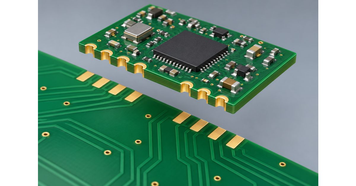
Table of Conent
Table of Conent
Castellated holes let a small PCB module connect to a larger host board through plated contacts along its edge. They can support a compact assembly without a separate header, but the module and host footprint must be designed together. A well-drawn module outline alone does not establish that the solder joints, panelization, or inspection plan will work.
This guide focuses on the manufacturing handoff: how to describe the edge contacts, coordinate the host pads, review assembly conditions, and prepare a clear RFQ. It avoids universal hole-size and pad-size rules because the appropriate geometry depends on the chosen fabrication and assembly processes.
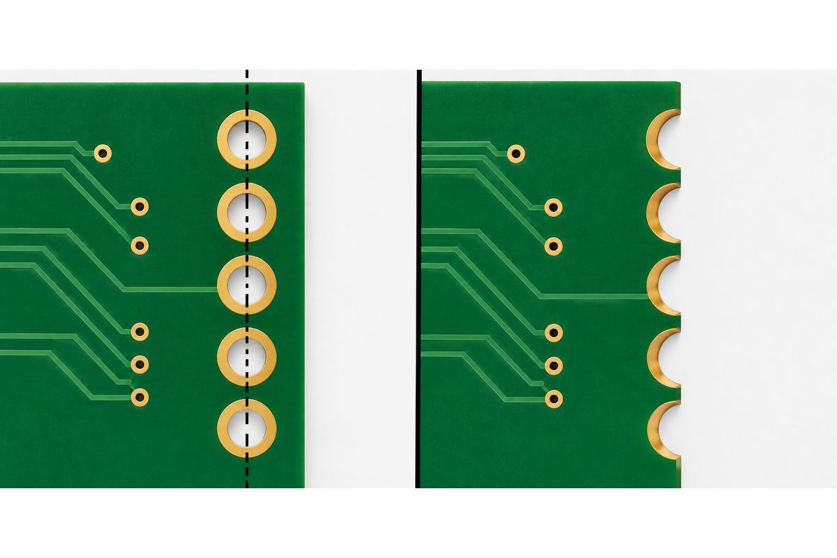
Understand the plated half-hole structure
A typical castellation begins as a plated hole that intersects the intended board profile. Profiling cuts through the hole, leaving an exposed plated section at the edge. Eurocircuits describes this manufacturing approach in its castellated PCB edge overview. Its published dimensions are recommendations for its own process, not a general capability statement for another supplier.
For a custom module, specify the intended finished geometry and identify the affected edges. Make the drawing clear enough that the fabricator can distinguish an intentional castellation from a plated hole accidentally placed too close to the outline. Confirm the proposed process and acceptance requirements before releasing a quantity build.
Coordinate the module contact and board profile
Review the finished-hole geometry, copper pads, edge position, and their tolerances as one construction. The remaining contact must support the intended electrical connection and assembly joint. Ask the fabricator to assess the proposed dimensions rather than reducing the hole or pad size simply to fit more contacts into the same edge length.
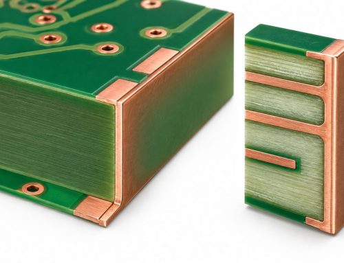
Identify the copper-layer treatment around the contacts and resolve any uncertainty in the fabrication data. For a multilayer module, the layer relationships need their own review. A feature that looks correct on the outer layers may still require clarification in the internal copper or production route.
Keep unrelated copper clear of the board profile according to the agreed rules. Intentional edge contacts should be called out explicitly, while other traces should not be treated as exceptions merely because they are nearby. Record approved changes to the geometry so the released files and drawing remain consistent.
Represent intentional edge contacts in the CAD data
Use the design tool’s appropriate pad and fabrication properties where available. For example, the KiCad PCB Editor documentation distinguishes castellated pads that intentionally intersect the board edge. Such properties help describe design intent, but they do not replace supplier review of the final exported files.
Inspect the Gerber and drill package after export. Check that the profile passes through the intended contacts and that the layer and hole information agrees with the fabrication drawing. Do not assume a clean editor preview proves that the manufacturer will interpret the production package in the same way.
If you import a footprint or reuse an older module outline, review its dimensions and orientation against the current design. A library feature can carry assumptions from another fabrication process. Keep the original reference information available and document any changes you make for the new build.
Design the host footprint from the actual module
The host board needs a controlled land pattern, not a visual approximation of the module edge. Coordinate pad locations, solder-mask openings, placement orientation, and the module’s assembled position. Where the module supplier provides a recommended pattern, use that as the starting point and evaluate any proposed changes.
Module-specific requirements can extend beyond the edge contacts. Espressif’s ESP32-WROOM-32E and 32UE documentation, for example, includes land patterns and module-placement guidance. The relevant drawing and keepout requirements belong to the selected part; a generic castellated footprint does not establish compatibility with every module.
Review clearance beneath and around the module. Account for the actual component heights, underside features, and product enclosure. Identify areas that must remain free of host components or copper according to the module requirements. An electrical connection table and mechanical placement drawing should describe the same orientation.
Plan panel support and separation early
Discuss panelization before filling every edge with contacts. The fabricator and assembler need a workable way to support the boards through production and separate them without compromising the intended contact areas. Ask where support features and separation operations can be accommodated on the proposed outline.
Review both the module panel and the host-board panel where they are part of the assembly scope. Their handling requirements may differ. The module needs a suitable presentation for placement, while the host assembly needs support through soldering and subsequent operations.
The PCB panelization guide explains why handling features belong in the manufacturing discussion. For castellated modules, include the edge-contact locations and assembly sequence when requesting the panel review.
Agree on the assembly process and soldering scope
Define whether the supplier will deliver bare modules, populated modules, or completed module-on-host assemblies. These are different work packages. If the module has already been assembled, obtain its handling and soldering requirements before planning another soldering operation on the host.
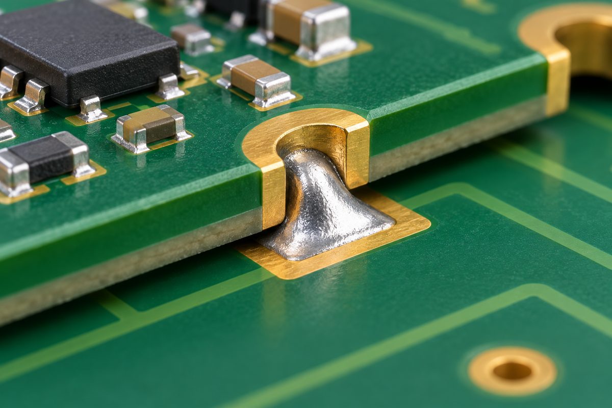
Ask the assembler to review the host land pattern and paste or soldering plan for the selected module. The target is a repeatable connection under the agreed process, not simply the largest visible solder deposit. Where a module has additional bottom pads or other hidden connections, include those features in the assembly and inspection discussion.
Identify nearby through-holes, copper features, and components that could affect the proposed joint. If the layout combines edge contacts with optional header positions, ask how the assembler will control the soldering operation and verify the intended connections. Avoid assuming the same footprint will behave identically under every assembly method.
Preparing a module build? Send the module fabrication data, host footprint, assembly drawing, quantity, and soldering requirements through the PCB engineering and quotation request. State which boards and assembly operations are included so the engineering review can assess the complete scope.
Define inspection evidence for the module and host
Agree on the requirements for the exposed contacts before manufacture. Ask how edge quality, plating condition, dimensions, and electrical connectivity will be evaluated. A feature that appears unusual should be compared with the agreed specification rather than accepted or rejected solely from an unscaled photograph.
For the assembled product, separate visual inspection from functional verification. Visible edge joints may support inspection, but they do not prove every circuit function or hidden connection. Define which checks establish placement, electrical connection, programming, and the behavior required by the application.

Keep inspection records traceable to both board revisions and the module identity. When a prototype reveals a problem, preserve representative samples and describe the observed condition clearly. A proposed cause should be supported by evidence before the design or production process is changed.
Release a complete manufacturing package
Supply the module Gerber and drill files, fabrication drawing, material and thickness requirements, surface finish, quantity, and schedule. Mark the castellated edges and the critical geometry. Include a netlist or other agreed electrical-test information where applicable to the fabrication order.
For module-on-host assembly, add the host manufacturing data, BOM, placement coordinates, and assembly drawing. Identify the module as a controlled item and clarify whether it will be supplied by you or sourced as part of the order. State approved substitutions, programming requirements, and test expectations.
The PCB manufacturing-release checklist explains the importance of synchronized exports and assembly documents. Apply that discipline to both boards so a revised host footprint is not paired with an outdated module.
Compare the requirements with the PCB manufacturing capabilities, then flag the edge-contact construction for project-specific review. A general capabilities page is a starting point; it does not by itself establish that a particular castellation geometry has been approved.
When requesting a combined build, submit these files and the sourcing, assembly, and inspection scope through the module fabrication and assembly quote request. The review can then address open manufacturing questions and prepare a relevant quotation.
Evaluate the prototype before committing to volume
Use the first build to verify module fit, placement orientation, soldering access, and the intended electrical functions. Include the real host and mechanical environment in that evaluation. A successful standalone module test does not establish that the integrated assembly satisfies the product requirements.
Record any changes to pads, profile geometry, assembly instructions, or inspection criteria. Review those changes with the supplier before issuing the next revision. Keep the approved module and host documents together so purchasing and production can identify the intended combination.
Conclusion
Castellated-hole PCB design is a coordination task between the module, host, fabricator, and assembler. Define the edge construction, use a controlled host footprint, provide a workable panel plan, and agree on assembly and inspection requirements. Those inputs make a compact module interface easier to manufacture consistently.
Ready for the next build? Submit the module and host files, quantity, schedule, and assembly and testing requirements through the online PCB RFQ form for an engineering and quotation review. Identify the critical edge contacts so the proposed manufacturing route can be evaluated against the actual design.
Latest Blog

Contact Info
Phone: +86-755-82882936
Email: [email protected]
WhatsApp: +86-13570802455
Wechat: +86-13570802455
Address: 2nd floor,D Bldg.,Electric Link Technology Bldg.,Gongming,Guangming New Dist.,518106 Shenzhen, China