
PCB Thickness Selection: Tolerances, Connector Fit, and Stackups
Table of Conent
Table of Conent
PCB thickness connects the electrical stackup to the mechanical product. A board can meet its nominal thickness target and still create an assembly problem if the connector, enclosure, or mounting hardware requires a tighter finished range. Conversely, choosing a thin board solely to save space can make handling and support more demanding.
The useful starting point is a clear definition of the finished thickness, the permitted variation, and the interfaces that depend on it. This guide explains how to make those decisions and communicate them in a fabrication request without imposing unnecessary restrictions.
Define which thickness you mean
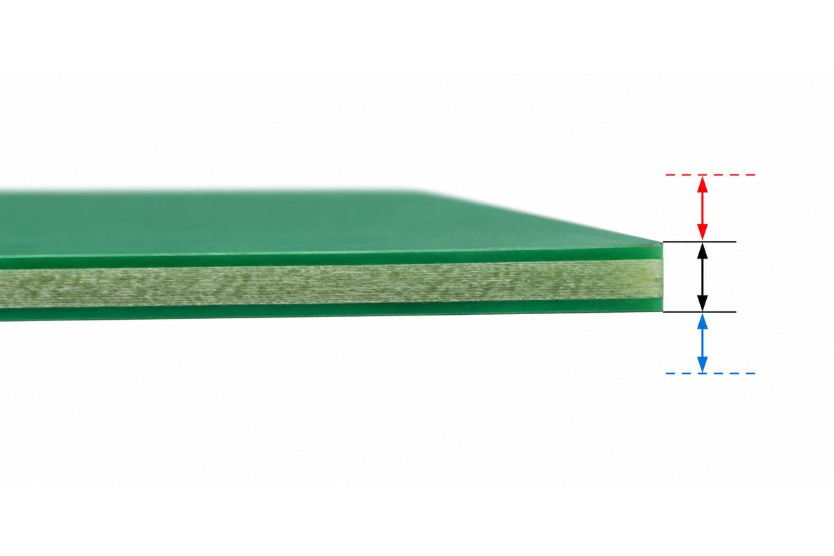
In a board drawing, thickness can refer to the laminate substrate, the finished bare board, or a local region such as a connector contact area. These values are related but are not interchangeable. Copper, plating, surface finish, and solder mask can affect the measurement, depending on where and how it is taken.
Write the requirement with its measurement basis. If a mechanical interface depends on the complete board thickness at a particular region, identify that region and whether the measurement includes the local surface layers. If the supplier proposes a stackup, confirm that its stated overall dimension uses the same basis as your drawing.
Keep the board thickness separate from the populated assembly height. Component bodies, solder joints, connectors, and attached hardware may dominate the height budget. A thinner substrate does not necessarily reduce the assembled product height by the amount the mechanical team expects.
Nominal thickness is only part of the requirement
A nominal dimension names the target; the tolerance defines the acceptable range. For example, a hypothetical requirement of 1.60 mm ±0.10 mm permits 1.50–1.70 mm. This example is arithmetic, not a recommended industry tolerance or a claim about supplier capability. The appropriate range comes from product fit and the qualified construction.
Do not assume that a supplier default tolerance is compatible with an edge connector or a tight enclosure slot. Ask for the expected finished range and compare both extremes with the mating hardware. When a tolerance is critical, put it in the fabrication drawing and RFQ rather than leaving it in an email that may not follow the order.
Let mechanical interfaces set the first constraints
Check enclosure rails, screws, standoffs, edge connectors, and press-fit components before finalizing the stackup. Each interface can constrain a different part of the board. A screw assembly may depend on the distance between supported surfaces, while an edge connector depends on the contact region thickness and geometry.
Connector requirements are product-specific. For instance, the Molex Sliver connector listing for part 2066530168 identifies a 1.57 mm PCB thickness. That value belongs to the named connector and should not become a general rule for every card-edge connector. Consult the selected part drawing and application specification for the full tolerance and contact requirements.
Also review bevels, plating, keepouts, and insertion direction. An overall thickness that fits does not establish that the contact geometry is correct. Coordinate the connector drawing with the fabrication data so the supplier can identify manufacturing questions before the first build.
Match the stackup to the electrical design
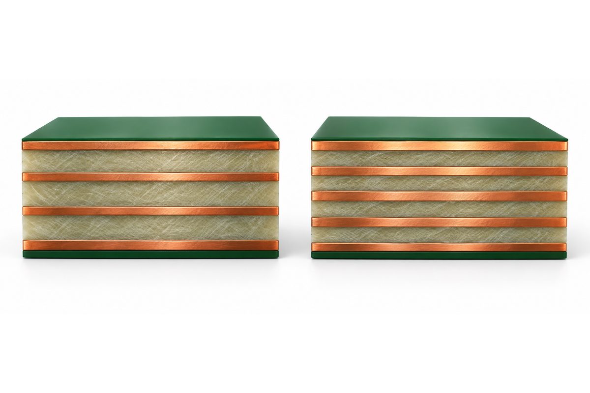
Overall thickness does not uniquely define a multilayer stackup. Two boards with the same finished thickness can have different core thicknesses, prepreg combinations, copper weights, and distances between signal layers and reference planes. Those differences matter to controlled impedance and routing decisions.
Work from the required layer functions and electrical constraints, then reconcile the proposed construction with the mechanical thickness range. For controlled-impedance nets, specify the target, tolerance, signal layer, and reference plane. Ask the fabricator to confirm the dielectric construction used for the calculation instead of accepting an overall dimension as sufficient detail.
The multilayer PCB design and production guide provides context for organizing a layer stack. For thickness selection, the next step is to review the actual construction and the constraints it must satisfy.
Why the fabrication review matters
A stackup is assembled from available materials and then processed. Isola’s laminate and prepreg overview describes bonding copper and prepreg through controlled lamination. For an individual design, the supplier must evaluate how the materials and artwork produce the required finished construction.
A calculated stack thickness should be treated as a planning value until the fabricator confirms it. The material combination, copper distribution, and production route need to support both overall thickness and dielectric requirements. A tighter tolerance may require additional review or a different construction; discuss the implications before freezing the design.
The PCB lamination and process-control guide explains why resin flow and copper distribution belong in this conversation. Thickness is one acceptance characteristic of a complete build, rather than an isolated purchasing option.
Balance space savings with handling needs
A thinner board can help meet a constrained product envelope, but the assembly and mechanical teams should review its support requirements. Large unsupported spans, panel handling, depanelization, and connector insertion loads deserve attention. The correct answer depends on board size, construction, component placement, and loading conditions.
Consider where the product supports the board and how it is handled during assembly. A design that is stable inside its enclosure may still need a carrier or additional panel support on the production line. Agree on the handling plan before ordering prototypes if it will influence panel geometry or component placement.
A thicker board is not automatically a better choice either. It consumes enclosure space, affects connector compatibility, and changes the drilling and stackup review. Choose the thickness that satisfies the defined interfaces and electrical construction, then evaluate manufacturing consequences.
Prepare a thickness-ready RFQ
Send complete fabrication data, the outline, drill files, quantity, and schedule. Include a drawing that identifies nominal finished thickness, tolerance, and any local region with a separate requirement. Provide the intended stackup, copper weights, material constraints, and controlled-impedance table when applicable.
If a connector sets the thickness range, identify its exact part number and relevant drawing. Flag whether the supplier may propose an alternative material combination or tune the stackup. If the outline or mounting design is still changing, say so; those changes can invalidate an earlier fit review.
Before requesting a quote, compare the design with the PCB manufacturing capabilities and identify requirements that need engineering clarification. Published information is a starting point; the released design still needs its own review.
Have a thickness-sensitive design ready for fabrication? Submit Gerber or ODB++ data, the drawing, stackup, quantity, and mating requirements through the PCB engineering and quotation request. These inputs allow the review team to assess the construction and prepare a relevant quote.
Agree on inspection before the build
When comparing thickness options, ask the supplier to explain the effect on material availability, tooling, inspection, and schedule. Request alternatives against the same electrical and mechanical requirements so the quotations are comparable. A lower nominal thickness or a tighter tolerance should earn its place through a product need, not an assumption that it will automatically improve cost or quality. Record which requirements are fixed and which are open to an engineering proposal.
Define how a critical thickness will be verified. Agree on the measurement location, surface condition, instrument, and sampling expectation where these affect acceptance. A measurement over copper or solder mask should not be compared casually with one taken on an exposed substrate region.
Separate thickness from flatness and warpage. A board may meet a thickness range yet have a shape that creates a handling or mating problem. If the product requires a separate planarity limit, identify that requirement explicitly rather than expecting the thickness note to cover it.
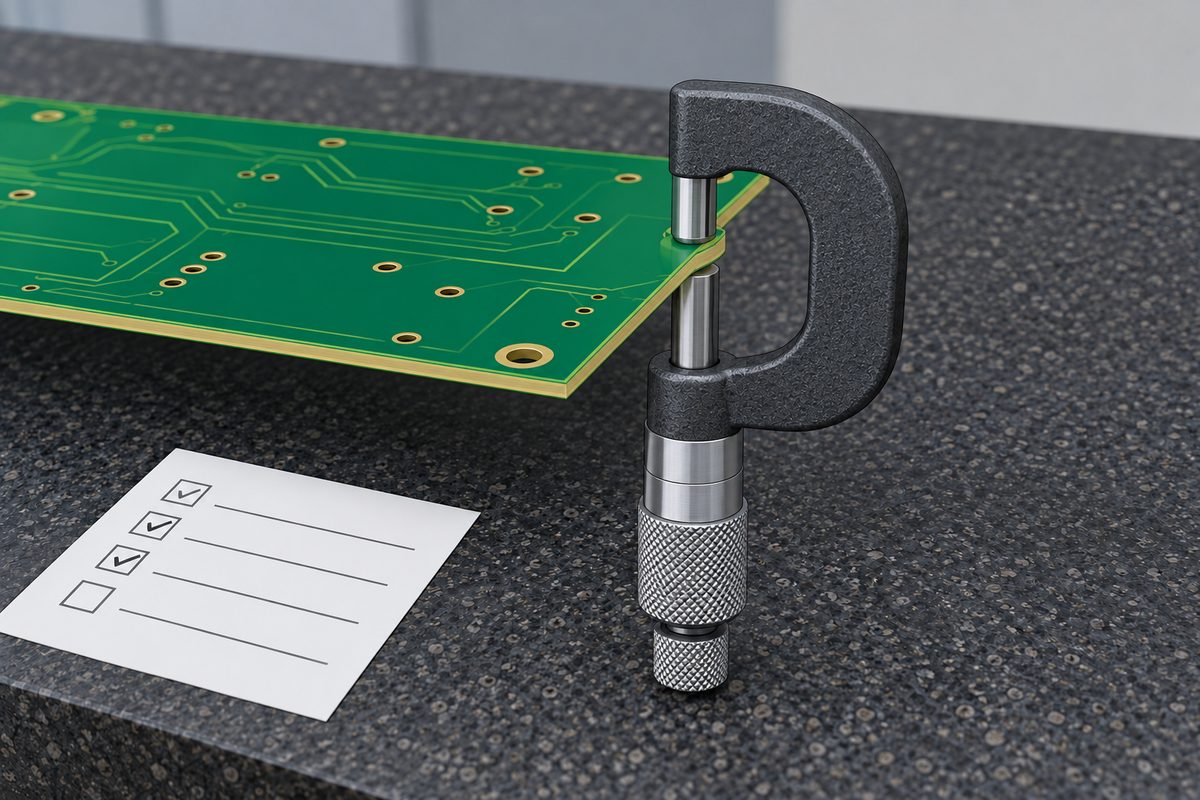
For prototypes, verify the critical interface with representative hardware before treating the design as production-ready. Record the board revision, measurement basis, and mating-part revision so the result can be traced. A successful fit check is evidence for that combination; later stackup or connector changes should trigger another review.
If the requirement remains unresolved, include it in the fabrication quote request with the relevant drawings. Ask for engineering review of the finished range and inspection expectations before production assumptions are finalized.
Keep thickness decisions under revision control
A material substitution, added copper layer, or revised connector can change the original thickness decision. Update the fabrication drawing, stackup, and mechanical model together. When the supplier proposes a change, check both the nominal value and tolerance against the approved interfaces instead of reviewing only the new material name.
For repeat orders, reference the approved construction and note which substitutions require review. Keep prototype fit results with the matching documentation revision. This gives purchasing and production a shared basis for evaluating changes and prevents an old nominal dimension from being reused after the design has evolved.
Conclusion
PCB thickness selection works best when mechanical interfaces, electrical stackup, and manufacturing review use the same definition. Specify a finished range, identify critical local regions, and confirm the construction with the fabricator. This helps avoid fit disputes and unnecessary restrictions while preserving requirements that matter.
Starting the next build? Send the released files, stackup, thickness requirements, quantity, and schedule through the online PCB RFQ form for an engineering and quotation review. Include mating drawings so the proposed construction can be evaluated against its real interfaces.
Latest Blog

Contact Info
Phone: +86-755-82882936
Email: [email protected]
WhatsApp: +86-13570802455
Wechat: +86-13570802455
Address: 2nd floor,D Bldg.,Electric Link Technology Bldg.,Gongming,Guangming New Dist.,518106 Shenzhen, China