
Carbon-Ink PCBs: Contact Design, Applications, and Manufacturing
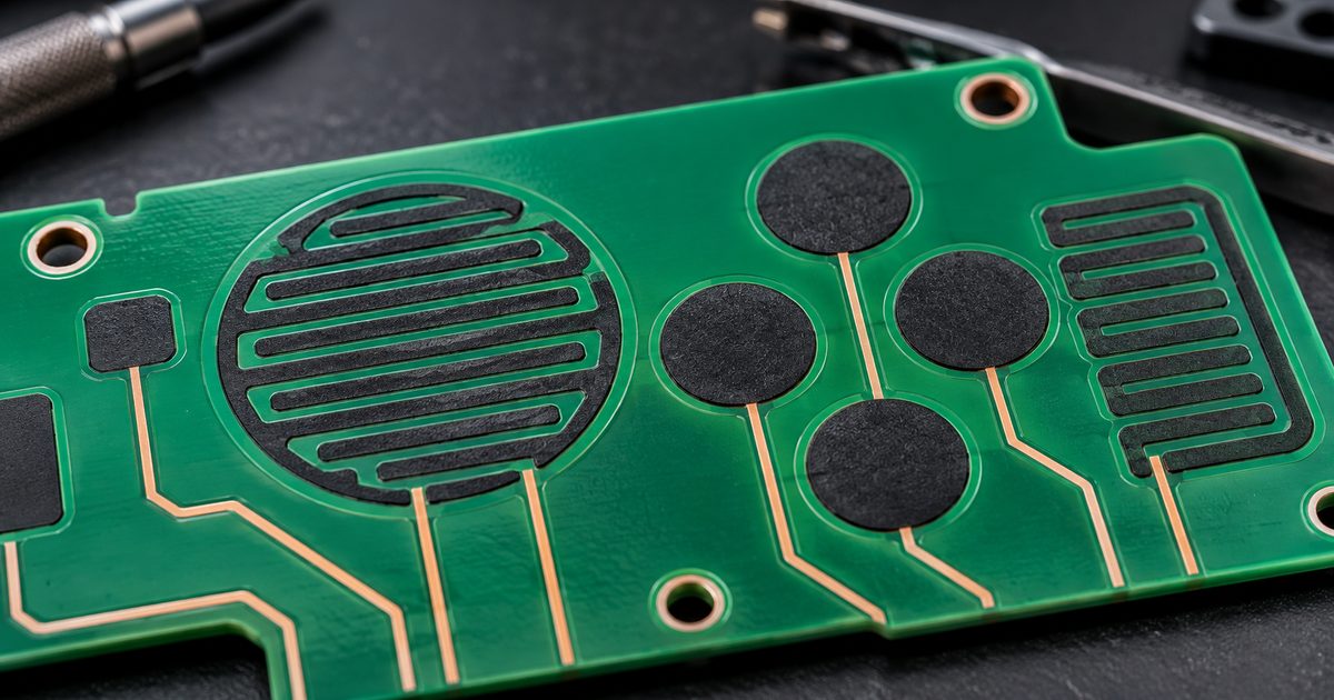
Table of Conent
Table of Conent
Carbon ink gives a printed circuit board a functional surface that ordinary solderable copper cannot always provide. A fabricator can screen-print a carbon-filled polymer over selected copper features to create keypad contacts, sliding contacts, low-power resistor elements, or protective contact surfaces. The result is usually less expensive than a precious-metal contact system, but it is not a drop-in substitute for hard gold, ENIG, or bare copper.
The engineering question is not simply whether a board can receive a carbon print. The drawing must define what the carbon feature does, which copper it overlaps, the resistance or continuity requirement, the mechanical interface, and the inspection method. Those choices affect artwork, solder mask, print registration, curing, assembly sequence, and final test.
What Is a Carbon-Ink PCB?
A carbon-ink PCB is a rigid or flexible circuit board with selected conductive features formed from a polymer thick-film ink containing carbon particles. The ink is deposited in a controlled pattern, normally by screen printing, and then cured according to the ink supplier’s process window. Depending on the material and geometry, the printed feature can act as a contact surface, a resistive element, or a bridge between conductive areas.
Carbon is useful because it resists oxidation at exposed contact surfaces, tolerates repeated low-energy mechanical actuation, and can provide a specified sheet resistance. It also introduces more electrical resistance than copper or plated metal. That difference is central to the design: carbon ink works well for signal-level contacts and resistive functions, but it is generally not the right choice for high-current connections or low-loss power paths.
The carbon layer is only one part of the interface. Copper geometry carries the signal into the printed area. Solder mask controls the opening and helps isolate adjacent features. The mating component—a silicone keypad pill, spring contact, wiper, or test interface—determines the pressure and wear pattern. A reliable design treats those elements as a system.
Where Carbon Ink Is Used on Circuit Boards
Keypad and membrane-switch contacts
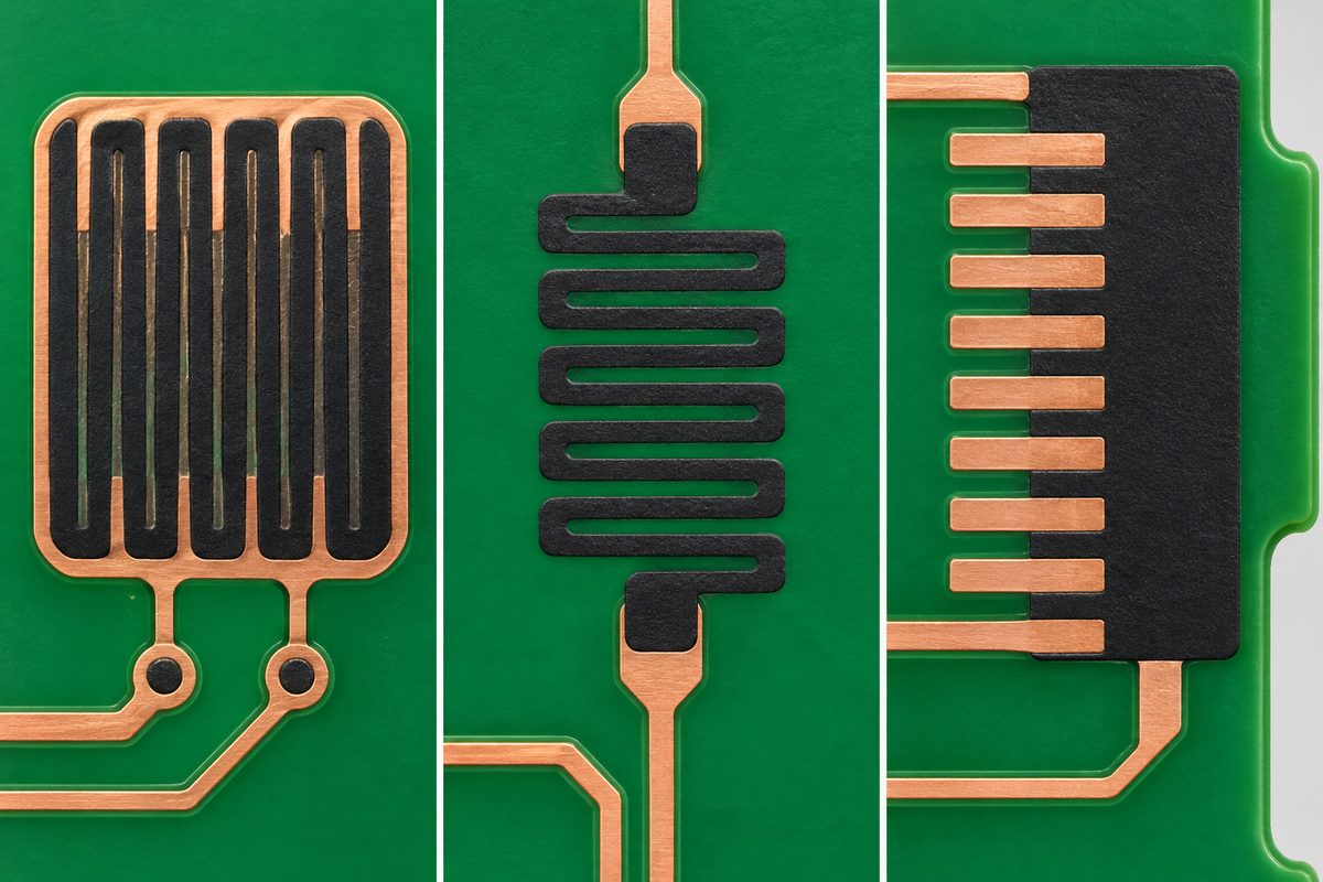
Interdigitated copper fingers covered by carbon ink are common under rubber keypads and membrane-switch domes. Pressing the conductive element bridges the separated fingers and closes the circuit. The layout must balance contact area, finger spacing, contamination tolerance, and the force delivered by the keypad.
Sliding and rotary contacts
A carbon overprint can provide a wear surface for low-energy wipers in controls, selectors, and position-sensing mechanisms. These applications need special attention to abrasion, contact pressure, travel path, debris, and the required resistance stability across the product life.
Printed resistors and jumpers
Because carbon ink has measurable sheet resistance, a printed track can serve as a resistor or a limited conductive link. Resistance depends on ink formulation, cured thickness, track length, track width, and process variation. A designer should therefore specify the required electrical result and tolerance rather than assuming that a nominal drawing geometry will create the same value with every approved ink.
Protective low-current contact areas
Carbon can protect selected copper features from direct handling or environmental exposure in cost-sensitive products. It should not be described as a universal replacement for a plated surface finish. Solderability, bondability, contact resistance, wear, and storage behavior differ among carbon, hard gold, ENIG, OSP, immersion tin, and other finishes.
How the Contact Stack Works
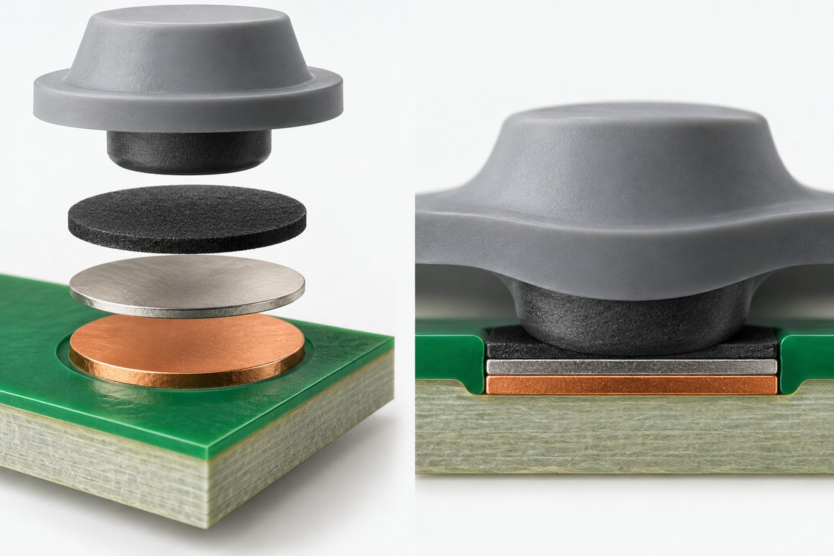
The base construction may be a simple single-sided board or part of a more complex multilayer design. For cost-sensitive controls, the principles in this 1-layer PCB design and manufacturing guide are a useful starting point. The carbon feature is added only where the functional interface requires it.
The copper underprint establishes electrical continuity and provides an adhesion surface. The required overlap between carbon and copper must tolerate print registration variation. If the overlap is too small, a shifted print can narrow the conductive connection or expose a vulnerable transition. If the carbon image extends too far, it can invade solderable pads, mask dams, board edges, or adjacent contacts.
The solder mask opening also needs deliberate control. Carbon should not be allowed to wander across an undefined mix of copper, finish, mask, and bare laminate. The fabricator should confirm which surfaces the selected ink is qualified to contact and whether an intermediate finish is compatible with printing and curing. Ink supplier data, such as the published processing information for DuPont BQ242 polymer thick-film carbon ink, illustrates why material-specific cure and application requirements matter.
Design Rules to Resolve Before Release
Define the function and electrical limit
State whether each feature is a switch contact, wiper track, resistor, jumper, or protective overprint. Then define the measurable requirement. For a switch, that may include closed-circuit contact resistance and insulation between open fingers. For a resistor, specify nominal resistance, tolerance, operating voltage, and any environmental or life-test conditions that matter.
Use a dedicated artwork layer
Provide a clearly named carbon-ink Gerber or equivalent fabrication layer. Do not encode carbon regions only in a PDF note or rely on a fabricator to infer them from copper geometry. The fabrication drawing should connect that layer to the material, cure, inspection, and acceptance notes.
Control overlap and clearance
Show the intended carbon-to-copper overlap, clearance to adjacent conductors, separation between independent carbon regions, and distance from routed or scored edges. The exact minimums depend on the fabricator’s printing process and the approved ink system. Ask for repeatable production tolerances rather than copying generic values from an unrelated supplier.
Separate carbon contacts from soldering areas
Carbon ink is not a solder mask and should not unintentionally cover component pads. Keep stencil openings, solder paste, flux, and hand-soldering operations away from functional contact surfaces. If the board will be assembled after carbon printing, agree on handling and cleaning controls so the contact region is not contaminated.
Design the mating mechanics with the PCB
For a keypad, check the pill diameter, travel, force, alignment tolerance, enclosure support, and the board’s ability to resist flexing. For a wiper, define the path, pressure, surface smoothness, and end stops. A sound electrical pattern can still fail if the enclosure applies uneven pressure or lets the contact land partly outside the printed region.
Plan test access
Add test points or accessible terminations that allow the finished contact circuit to be measured without probing and damaging the working surface. Coordinate this with the broader PCB assembly and quality-control process, especially when functional testing must exercise the keypad or sensor after component placement.
If your drawing currently shows only a black contact area without material, resistance, overlap, or inspection requirements, send the Gerber data, fabrication drawing, mating-contact details, quantity, and acceptance criteria through the PCB quote and engineering review form. The review should resolve the print definition before production artwork is released.
Carbon-Ink PCB Manufacturing Flow
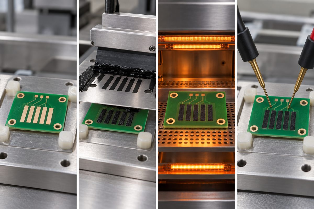
- Data and material review. The fabricator checks the carbon artwork, base construction, copper and solder-mask geometry, surface finish, material compatibility, and acceptance requirements.
- PCB fabrication. Copper imaging, etching, drilling, plating, solder mask, and relevant surface-finish operations create the underlying board. The exact sequence depends on the construction.
- Surface preparation. The print area must be clean and compatible with the ink. Contamination or oxidation at the interface can affect adhesion and electrical consistency.
- Screen printing. A controlled screen, stencil, squeegee setup, and ink condition define the printed image and wet-film deposit.
- Curing. Time and temperature follow the approved ink system and board limitations. Under-cure can compromise adhesion or resistance; excessive heat can affect the laminate, finish, or solder mask.
- Inspection and test. Typical checks may include visual coverage, registration, adhesion, thickness or sheet resistance where applicable, circuit resistance, insulation, and application-specific contact tests.
- Protected handling and packing. Finished contact surfaces should be kept free of oils, abrasive contact, dust, and packaging materials that can transfer residue.
Carbon printing must fit the complete fabrication route, not sit outside it. The discussion of data control, imaging, etching, finish, testing, and packing in this overview of PCB fabrication process and supplier criteria also applies to carbon-enhanced boards. The added print step creates another controlled material and another inspection gate.
How to Specify a Carbon-Ink PCB in an RFQ
A useful request for quotation should include:
- Gerber, ODB++, or IPC-2581 data with a dedicated carbon layer;
- fabrication drawing and stackup;
- board material, finished thickness, copper weight, and surface finish;
- carbon feature function and approved ink requirement, if material is controlled;
- resistance, continuity, insulation, adhesion, or wear acceptance criteria;
- mating-contact geometry, load, travel, and expected cycle conditions when relevant;
- panelization and keep-out requirements;
- assembly files and cleaning restrictions if components will be mounted;
- quantity, revision, traceability, packaging, and required inspection records.
Confirm that the supplier’s base-board range matches the design before discussing the special print. AssyPCB’s published PCB manufacturing capabilities provide a starting point for ordinary construction limits, but a carbon-ink requirement still needs project-specific engineering confirmation.
If the project includes component assembly, submit the BOM, centroid data, assembly drawing, approved alternates, and test instructions with the fabrication package. Use the quote upload to request a combined review of the carbon-contact board and the downstream PCBA process.
Inspection and Qualification Questions
A drawing should say how compliance will be demonstrated. Consider these questions during supplier review:
- Will resistance be measured on every board, by lot sampling, or with a process coupon?
- Where are the measurement points, and what probe force or fixture is appropriate?
- Does the contact require actuation testing with the real mating component?
- Are adhesion, abrasion, humidity, temperature cycling, or contamination tests required by the product environment?
- What visual defects are rejectable: voids, smearing, edge roughness, exposed copper, misregistration, or contamination?
- How will the supplier identify ink lot, cure record, PCB lot, and inspection record if traceability is required?
Do not apply a wear or environmental test simply because it appears in another product’s specification. Qualification should reproduce the relevant stresses of the actual interface. A handheld keypad, an industrial selector, and a printed calibration resistor expose the carbon feature to different electrical and mechanical risks.
Common Failure Modes and Preventive Actions
| Failure mode | Likely contributors | Preventive action |
|---|---|---|
| High or unstable resistance | Ink selection, print thickness, cure, narrow geometry, or contamination | Specify the electrical result, validate material and geometry, and control curing and cleanliness |
| Intermittent keypad response | Misalignment, insufficient contact area, board flex, or uneven actuator force | Review the PCB, keypad, enclosure, and support structure as one tolerance stack |
| Carbon-to-copper discontinuity | Insufficient overlap or print registration shift | Provide a defined overlap with manufacturing margin and inspect the transition |
| Peeling or cracking | Poor surface preparation, incompatible materials, incorrect cure, or mechanical strain | Qualify the ink/substrate system and keep flexing away from rigid printed contacts |
| Contaminated contact surface | Flux, cleaning residue, fingerprints, dust, or packaging transfer | Protect the area through assembly, cleaning, inspection, and packing |
| Premature wear | Excessive force, abrasive wiper, rough print, or unsuitable ink | Define the mating mechanics and run representative life testing |
Carbon Ink vs. Plated Contact Finishes
Carbon ink is attractive when the application accepts higher contact resistance and benefits from a printed, oxidation-resistant, low-cost functional surface. Hard gold is generally considered when a low-resistance, durable metal contact must withstand repeated mating or sliding, although thickness, nickel underlayer, geometry, and cost require control. ENIG provides a flat solderable surface and is useful for many assembly pads, but it is not automatically equivalent to hard gold for wear contacts.
The selection should follow the interface requirement rather than a simple price hierarchy. Ask what current and signal level the contact carries, how many cycles it sees, whether it slides or only presses, what contaminants are present, how tightly resistance must remain controlled, and whether the same area must also be soldered or wire-bonded.
Final Engineering Checklist
- The carbon feature has one clearly stated function.
- A dedicated fabrication layer defines every printed area.
- Copper overlap, mask opening, clearances, and mating geometry are documented.
- Electrical and mechanical acceptance criteria are measurable.
- The ink system and cure route are compatible with the board construction.
- Contact surfaces are protected from soldering, cleaning, handling, and packing contamination.
- Test access and traceability match the product risk.
- The PCB fabricator and assembler have reviewed the same controlled revision.
A carbon-ink PCB can combine simple board construction with a useful contact or resistive function, but reliable results depend on a precise interface specification. Prepare the carbon artwork, fabrication drawing, electrical limits, mating-contact details, quantity, and test expectations, then submit the project for fabrication and DFM review. The engineering review can confirm the build route, identify missing acceptance criteria, and return a quotation based on the actual contact system.
Latest Blog
Contact Info
Phone: +86-755-82882936
Email: [email protected]
WhatsApp: +86-13570802455
Wechat: +86-13570802455
Address: 2nd floor,D Bldg.,Electric Link Technology Bldg.,Gongming,Guangming New Dist.,518106 Shenzhen, China