
PCB Lamination: Materials, Process Controls, and Design Review
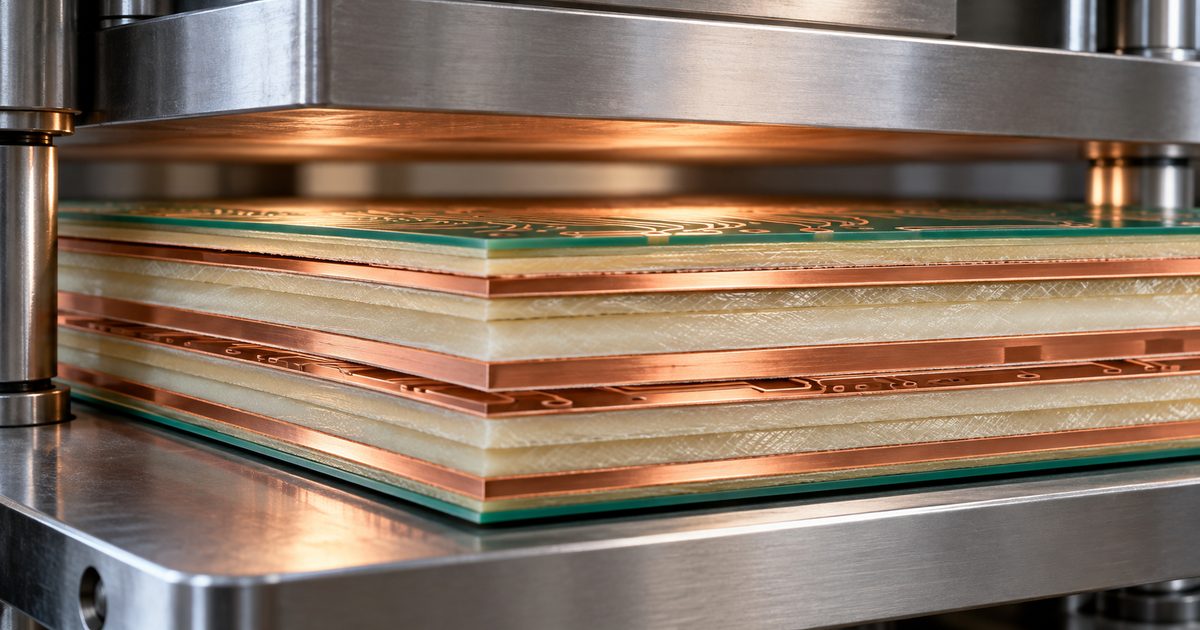
Table of Conent
Table of Conent
PCB lamination is the controlled bonding step that turns prepared copper circuits, dielectric layers, and prepreg into a stable multilayer board. It is easy to describe as “pressing layers together,” but that shorthand hides the decisions that influence finished thickness, dielectric spacing, registration, resin fill, and reliability. For a simple build, a fabricator can often apply a proven press program. For a dense or controlled-impedance design, the stackup, copper pattern, materials, and documentation need to agree before the job reaches the press.
This guide explains what designers and sourcing teams should specify, what the factory controls during lamination, and how to make a release package easier to manufacture. It focuses on practical review questions rather than treating lamination as an isolated factory operation.
What PCB lamination does
A multilayer board begins as a collection of prepared inner layers, copper foil, rigid dielectric cores, and partially cured bonding sheets called prepreg. Under a defined combination of heat, pressure, vacuum, and time, the resin in the prepreg softens and flows. It fills intended spaces, bonds the layers, then cures into the dielectric that separates copper planes and traces.
The resulting laminate must do several jobs at once: hold copper layers in their planned positions, provide electrical isolation, maintain the intended dielectric thickness, and remain mechanically sound through drilling, plating, assembly, and service. That is why lamination belongs in the early stackup conversation alongside layer count and routing density. A multilayer PCB design review is a useful starting point, but the final press package needs material and construction detail beyond a generic layer diagram.
Core, prepreg, and copper: the material relationship
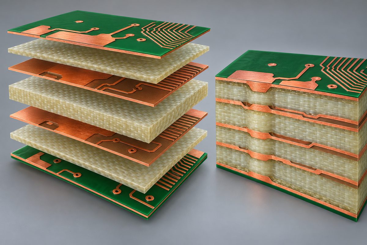
Core is a fully cured laminate with copper on one or both sides. It contributes a predictable dielectric thickness and is commonly used as the starting substrate for inner-layer imaging. Prepreg is reinforcing glass cloth impregnated with resin that has been partially cured. During pressing, it becomes the adhesive and dielectric between prepared layers.
Prepreg selection is not simply a matter of choosing a nominal thickness. Resin content, glass style, copper coverage, and the voids that need filling all change how much resin remains after pressing. Heavy copper, wide gaps, deep etched features, and uneven copper distribution may demand more resin flow than a balanced signal layer. Conversely, excessive flow can change dielectric thickness or create resin-rich areas where the design expected a tighter construction.
Ask the fabricator to evaluate the actual artwork and stackup rather than approving a material callout in isolation. A manufacturer may propose a qualified substitution or a revised prepreg combination to reach the required impedance and finished thickness; that decision should be documented against the electrical and mechanical requirements. The Isola laminate and prepreg processing guide similarly notes that a lamination cycle depends on stackup, complexity, thickness, and press capability.
Stackup decisions to close before CAM release
A good stackup answers more than “how many layers?” It identifies the intended order of copper and dielectric materials, nominal and tolerance targets, copper weights, controlled-impedance layers, and special constraints such as high-voltage spacing or low-loss material requirements. Before release, review the following points with the fabricator:
- Layer pairing and symmetry: Balanced construction can help limit bow and twist. When an asymmetric stack is necessary, flag it so the fabricator can assess compensation and process risk.
- Copper distribution: Large plane areas beside sparse routing change the resin demand. Copper balancing patterns or thieving may be appropriate, but they must not compromise impedance, isolation, or thermal intent.
- Dielectric targets: For impedance-controlled lines, name the reference plane, target impedance, tolerance, and applicable calculation assumptions. Do not assume that the prepreg’s catalog value equals the pressed dielectric thickness.
- Sequential builds: Blind, buried, or stacked microvias can require more than one lamination cycle. Show the build sequence explicitly so the factory can plan registration, drill, and plating stages.
- Material restrictions: State required Tg, thermal behavior, halogen restrictions, or approved laminate families when those constraints are real design requirements—not merely a copied note.
Not every board needs a complex construction. A well-scoped two-layer PCB may be more economical and easier to validate when it can meet the electrical and mechanical need. When a multilayer stack is justified, however, documenting the rationale gives the engineering review team a reliable baseline.
How the lamination process is controlled
The exact press recipe is factory- and material-specific, but a disciplined workflow follows a recognizable sequence. Inner layers are imaged, etched, inspected, treated for bonding, and prepared with tooling holes. The layup team then assembles cores, prepreg, copper foil, and release materials in the approved order. Registration tooling and optical targets help keep the copper features aligned before the panel enters a vacuum press.
During the press cycle, vacuum helps reduce trapped air while the temperature and pressure profile lets resin flow before final cure. The panel is then cooled in a controlled manner before it moves to downstream drilling, plating, and outer-layer work. A qualified process uses coupons, microsections, or other inspection evidence where appropriate to confirm bond quality, dielectric construction, and registration.
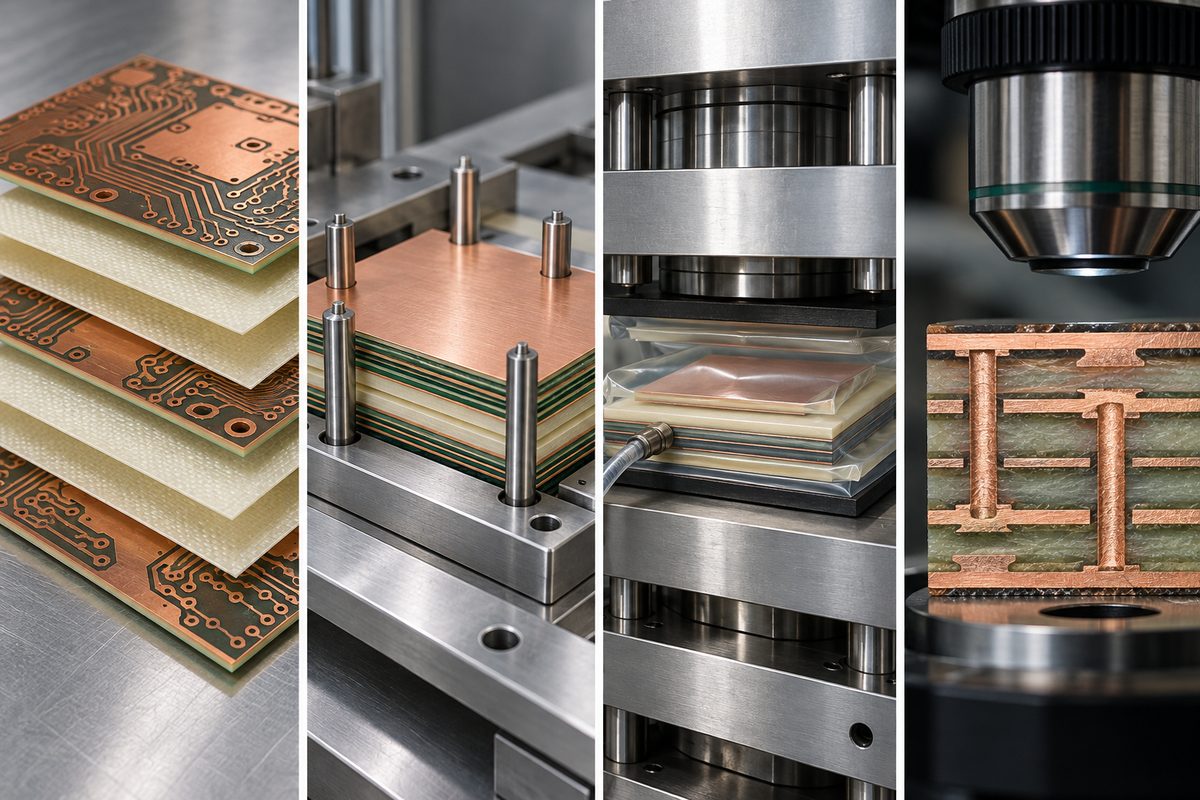
Press parameters are not transferable by guesswork between material systems. Resin chemistry, panel thickness, copper loading, and the number of layers affect heat transfer and flow. Give the fabricator room to use a qualified material-specific cycle, while keeping your acceptance requirements clear. For boards intended for demanding supply chains, ask what evidence will be available in the build record and how material lot traceability is handled.
Common lamination defects and what they signal
Most lamination problems trace back to a mismatch between design, material, handling, or process control. The following issues are worth discussing during DFM rather than discovering after electrical test or assembly:
- Voids or incomplete fill: trapped air, insufficient resin, poor surface preparation, or an unsuitable flow profile can leave unbonded areas. They can reduce dielectric integrity and weaken the structure.
- Resin starvation: a high-demand copper pattern or inadequate prepreg can leave too little resin in critical areas. This may expose glass weave or produce local dielectric variation.
- Delamination: contamination, moisture, weak oxide treatment, or inappropriate cure conditions can impair adhesion between materials.
- Misregistration: layer movement, tooling error, or dimensional change can shift pads and vias relative to their intended targets. Fine-pitch features and sequential builds require added attention.
- Thickness variation or warpage: unbalanced copper, asymmetric construction, and uneven flow can affect planarity and finished dimensions.
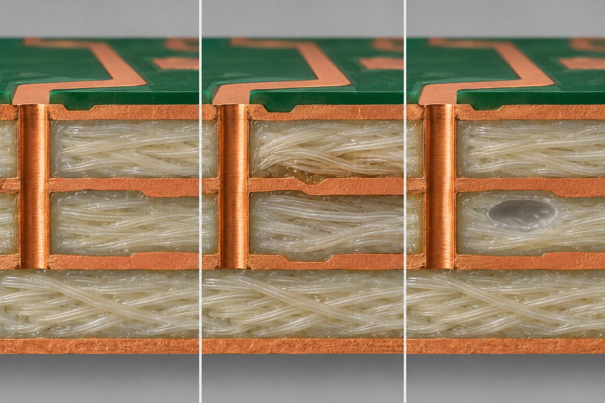
These labels are useful for a review, not a substitute for acceptance criteria. Define which specifications, coupon requirements, test methods, and reporting requirements apply to the order. When a particular standard or customer specification governs the build, include the revision and any agreed exceptions in the purchasing documentation.
Turn requirements into measurable acceptance evidence
Requirements are most useful when they can be inspected or tested at an agreed point in the build. For example, a finished board thickness target should include its tolerance and measurement location; an impedance requirement should identify the net classes, test coupon expectation, and acceptable tolerance; and a registration concern should be tied to the smallest annular-ring or feature relationship that makes it important. This prevents a review from relying on vague instructions such as “keep layers aligned” or “use standard material.”
For complex boards, ask whether the fabrication drawing should identify coupon locations, sectioning expectations, and any documentation to be returned with the shipment. The appropriate evidence depends on the product and contract: one job may only need routine electrical test, while another may require material records, cross-section review, or agreed first-article documentation. State the requirement before production begins so it can be incorporated into the route rather than requested after panels are complete.
It also helps to separate functional requirements from preferred construction. A specified laminate family can be essential when it supports a validated electrical or thermal design; in other cases, a measurable impedance, temperature, and thickness requirement may allow the fabricator to propose an available equivalent. Clarifying that distinction can reduce unnecessary sourcing delay while preserving the characteristics that matter to the finished product.
Finally, keep revision control visible. The fabrication drawing, stackup table, impedance note, and manufacturing data should identify the same revision. A late artwork change can alter copper distribution or clearance and may require the stackup review to be repeated. Sending a single, controlled release package makes it easier for the supplier to confirm that the press plan matches the design that will actually be built.
Make the RFQ package lamination-ready
The fastest route to an actionable lamination review is a complete release package. Supply Gerber or ODB++ data, drill files, fabrication drawing, stackup, netlist when available, quantity, panelization preference, finish, and test requirements. For controlled-impedance designs, include the target values, layers, reference planes, tolerance, and whether the supplier may tune trace width after stackup confirmation. For sequential lamination, show the build order and the via structure in a way that cannot be mistaken for a standard through-hole build.
Also call out the requirements that change material or press choices: finished thickness tolerance, copper weights, minimum dielectric spacing, thermal constraints, high-voltage clearance, reliability expectations, and approved material families. If schedule is critical, note the required delivery date and ask the manufacturer to identify material lead-time risk before release. Broader sourcing considerations are covered in this guide to PCB production planning.
What to ask during a supplier review
A useful review is a two-way engineering conversation. Confirm whether the proposed stackup is manufacturable with qualified materials, whether the copper distribution needs balancing, whether the impedance model uses pressed dielectric values, and whether any panel or artwork changes are needed for registration. For a build with special reliability needs, ask which inspection data can be supplied and which requirements need to be agreed before the purchase order.
If you need the board design checked against a practical stackup and manufacturing route, send the release package through the PCB quote form. Include the layer count, finished thickness, copper weights, target impedance, material constraints, quantity, and deadline so the engineering team can return a focused manufacturability review rather than a generic estimate.
For teams evaluating a new supplier or a higher-layer-count build, the PCB manufacturing capabilities page can help frame the questions to include in the request. Then use the quote request to share the actual design data and receive guidance tied to the requested construction.
Conclusion
PCB lamination is where a planned stackup becomes a physical, electrically functional structure. Clear material callouts, realistic dielectric targets, balanced copper, and a complete RFQ package give both the design team and the fabricator a better chance to prevent avoidable rework. Treat the press cycle as a qualified manufacturing control, and treat the design release as the information source that makes that control effective.
When your board needs an engineering review before fabrication, submit the stackup and production files through the online RFQ form. State the lamination-sensitive requirements up front so the proposed build can be reviewed against your actual performance and schedule needs.
Latest Blog
Contact Info
Phone: +86-755-82882936
Email: [email protected]
WhatsApp: +86-13570802455
Wechat: +86-13570802455
Address: 2nd floor,D Bldg.,Electric Link Technology Bldg.,Gongming,Guangming New Dist.,518106 Shenzhen, China