
PCB Edge Plating: Layer Connections, Panel Tabs, and RFQ Files
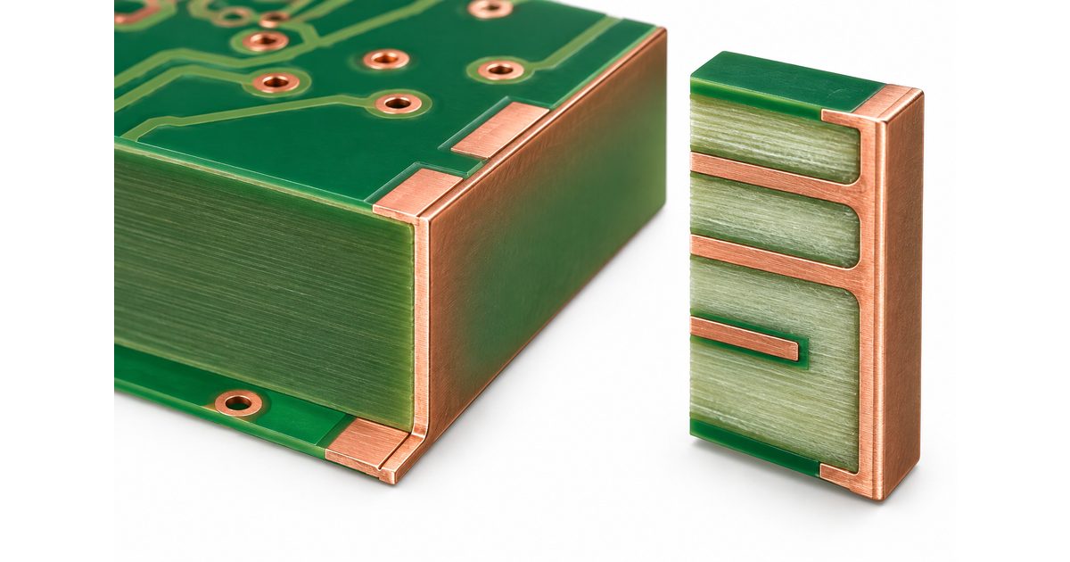
Table of Conent
Table of Conent
PCB edge plating adds a conductive metal coating to selected board sidewalls. It can provide a perimeter connection between specified copper layers or an interface to a shielding or contact arrangement. The design must define which edges are plated and which copper is allowed to connect to them. A line drawn at the board outline is not a complete fabrication instruction.
For engineers and buyers, the important decisions cross the electrical, mechanical, and manufacturing boundaries. This guide explains how to describe the connection, account for panel support interruptions, select an appropriate finish, and prepare a useful quotation package. It does not assume that a general PCB capability statement qualifies a particular edge-plating design.
Separate sidewall plating from other edge features
Edge plating, also called sideplating or edge metallization, coats an exposed board contour. It differs from a row of gold connector fingers on a board face and from plated half-holes used for solderable module connections. These features may appear near the same outline, but their intended contact geometry and fabrication requirements differ.
Eurocircuits’ round-edge plating explanation describes contour preparation before metallization and the need to identify the process in the order. This is a useful reminder that an ordinary final-profile operation does not automatically produce a plated sidewall.
If the design actually needs solder joints along a module edge, compare that requirement with the castellated-hole PCB design guide. Select the feature by the electrical and mechanical interface it must provide, not by whether its exposed copper looks similar in a photograph.
Define the electrical purpose before drawing the plated contour
State whether the coating provides a connection between specified ground layers, a contact area, or another defined interface. Identify the net and the exact layer connections. A phrase such as “plate all edges for shielding” leaves important questions unanswered about isolation, contact locations, and permitted interruptions.
Do not assume that edge plating alone guarantees an electromagnetic compatibility result. Shield performance depends on the full system, including enclosure interfaces, openings, cables, return paths, and the frequencies of interest. Treat the plated edge as one feature in that system and validate the relevant product requirement.
For a contact arrangement, define the mating part and the expected use conditions. A coating suitable for a solderable edge may not be the correct choice for repeated mechanical contact. Agree on the interface and its acceptance requirements before selecting a finish or asking a supplier to quote a generic plated perimeter.
Connect selected layers and isolate everything else
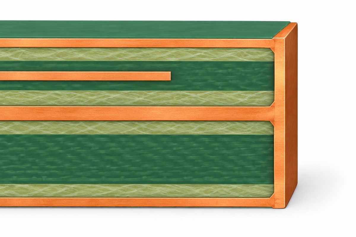
The layout must distinguish copper intended to meet the metallized contour from copper that must remain isolated. Review every affected layer, including planes, tracks, and exposed copper features. A signal trace too close to the plated sidewall can create an unintended connection even if the top-layer view looks correct.
WEdirekt’s PCB design guide provides a supplier-specific example of edge-plating connection and clearance requirements. Its dimensions describe that supplier’s defined process; they are not universal design rules or evidence of assypcb.com’s capabilities. Obtain confirmation for the actual construction being ordered.
Ask the fabricator how the plated contour should be represented in the copper and mechanical data. Confirm the required connection land and isolation clearance in writing. Check corners, nearby mounting features, and transitions between plated and unplated segments, where a simple straight-edge rule may not describe the complete geometry.
Account for panel support and unplated interruptions
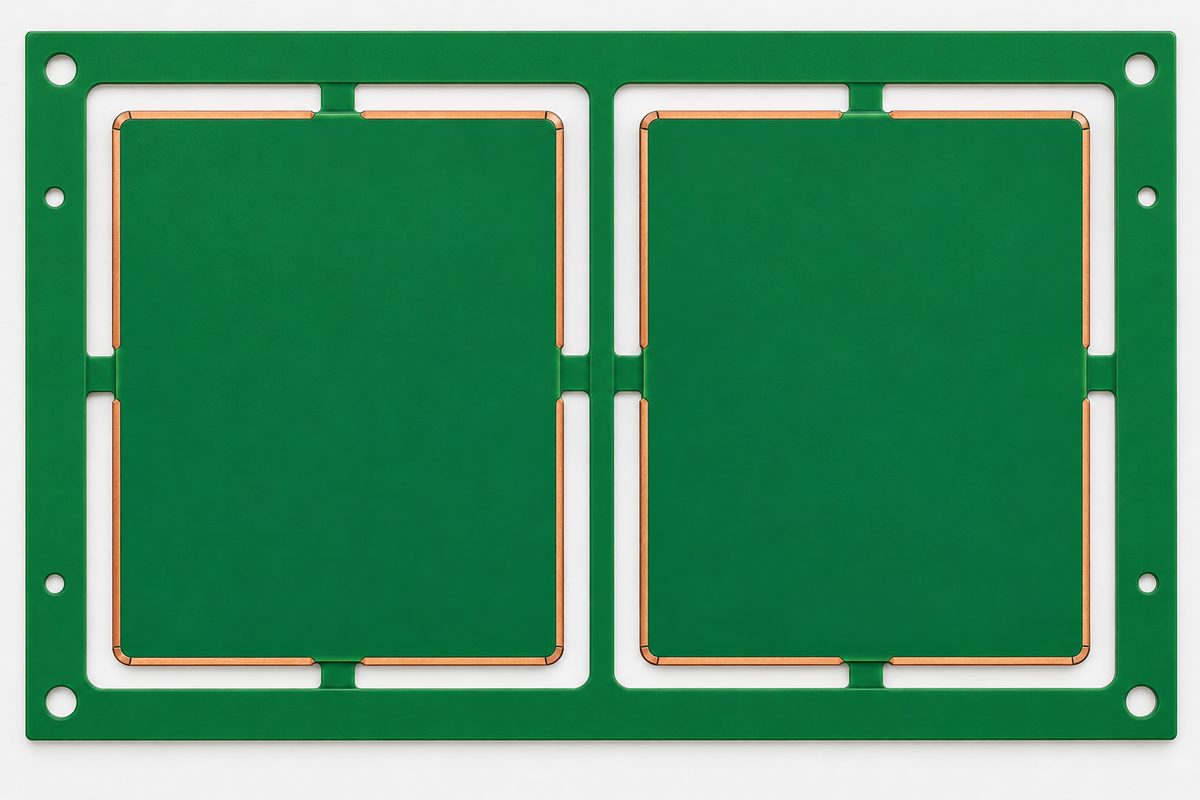
The manufacturer needs a way to hold the board during the relevant processing stages. Discuss how the chosen panel arrangement and support features affect the exposed contour. Do not specify an uninterrupted plated perimeter while also assuming that arbitrary support tabs can be placed anywhere on that perimeter.
Identify edge segments where an interruption is acceptable and those that serve a critical contact or shielding interface. Ask the fabricator to show the proposed support locations before approving the panel. If an interruption falls in a functional area, resolve the board or panel design rather than accepting a last-minute workaround.
The PCB panelization guide explains the broader role of rails and separation features. For an edge-plated board, panelization must also preserve the agreed metallized segments and the condition of those segments after separation.
Planning an edge-plated prototype? Send the board outline, layer data, stackup, required plated segments, quantity, and acceptable interruption locations through the PCB engineering and quotation request. Ask for review of the proposed connection, clearance, and panel-support approach before the order scope is finalized.
Choose the finish for the interface, not the appearance
Specify the required sidewall finish and discuss its compatibility with the proposed fabrication route. Do not infer a gold thickness or contact rating from the color of a sample. The finish must be evaluated against soldering, contact, environmental, or other requirements applicable to the feature.
Eurocircuits’ gold-finish guidance for edge connectors distinguishes ENIG from hard plated gold for connector fingers. That distinction helps explain why a generic “gold finish” note can be ambiguous. Connector-finger specifications should not be transferred automatically to sidewall plating.
Separate finish selection from solder-mask requirements. Identify any exposed lands, mask boundaries, and surfaces that must remain accessible to the mating interface. If coating, adhesive, or enclosure hardware will interact with the edge, include those conditions in the design review so an assembly operation does not obstruct the intended connection.
Release files that describe the entire feature
Provide the ordinary PCB manufacturing package and a controlled drawing that identifies the plated contour. Use a common board revision and coordinate reference. The drawing should distinguish plated segments from ordinary routed edges and state which layers or nets are intentionally connected.
Include the stackup, copper data, board outline, finish requirement, and relevant connection and clearance notes. Show acceptable support interruptions where they are part of the design. If a requirement is defined in another controlled document, reference that document rather than leaving the information in an informal purchasing message.
Review the data as a complete set. A mechanical drawing cannot repair copper that contradicts its isolation note, and a highlighted copper outline does not explain a missing finish requirement. Ask the supplier to identify discrepancies before production rather than infer which file takes precedence.
Ask for project-specific manufacturing confirmation
Use the PCB manufacturing capabilities as the starting point for the wider board design. Then obtain explicit confirmation of the edge-plating scope, including the selected contour, layer connections, finish, interruptions, and inspection requirements. A general page does not prove that a specific combination has been accepted.
Clarify who owns panel preparation and who approves its functional consequences. If the supplier proposes moving a support tab or changing the edge preparation, send the proposal to the responsible design owner. Purchasing should not approve a change to a critical contact area simply because the board still fits the enclosure.
For unresolved details, attach the current files and list the open connection, finish, or support questions in the edge-plated PCB quotation request. The engineering and quotation review can then separate agreed requirements from assumptions that still need approval.
Agree on inspection and test coverage
Define the visible condition and dimensional features that matter at the plated edge. Depending on the application, the review may include coverage of the specified segments, permitted interruptions, surface condition, and fit with the mating structure. Establish the acceptance interpretation and reporting scope with the manufacturer before the build.
Electrical testing can address intended connections and isolation included in its coverage. It does not automatically prove every coating property, contact-life requirement, or system shielding result. Match each requirement to the appropriate evidence and state which checks are required for the prototype and production orders.
Preserve inspection access in the sample plan. If a critical edge is hidden by an enclosure or assembly operation, decide when it will be evaluated and which records should be retained. Where a special evaluation affects the sample, allocate it deliberately rather than using a board already committed to another validation task.
Keep quotation and repeat-order assumptions visible
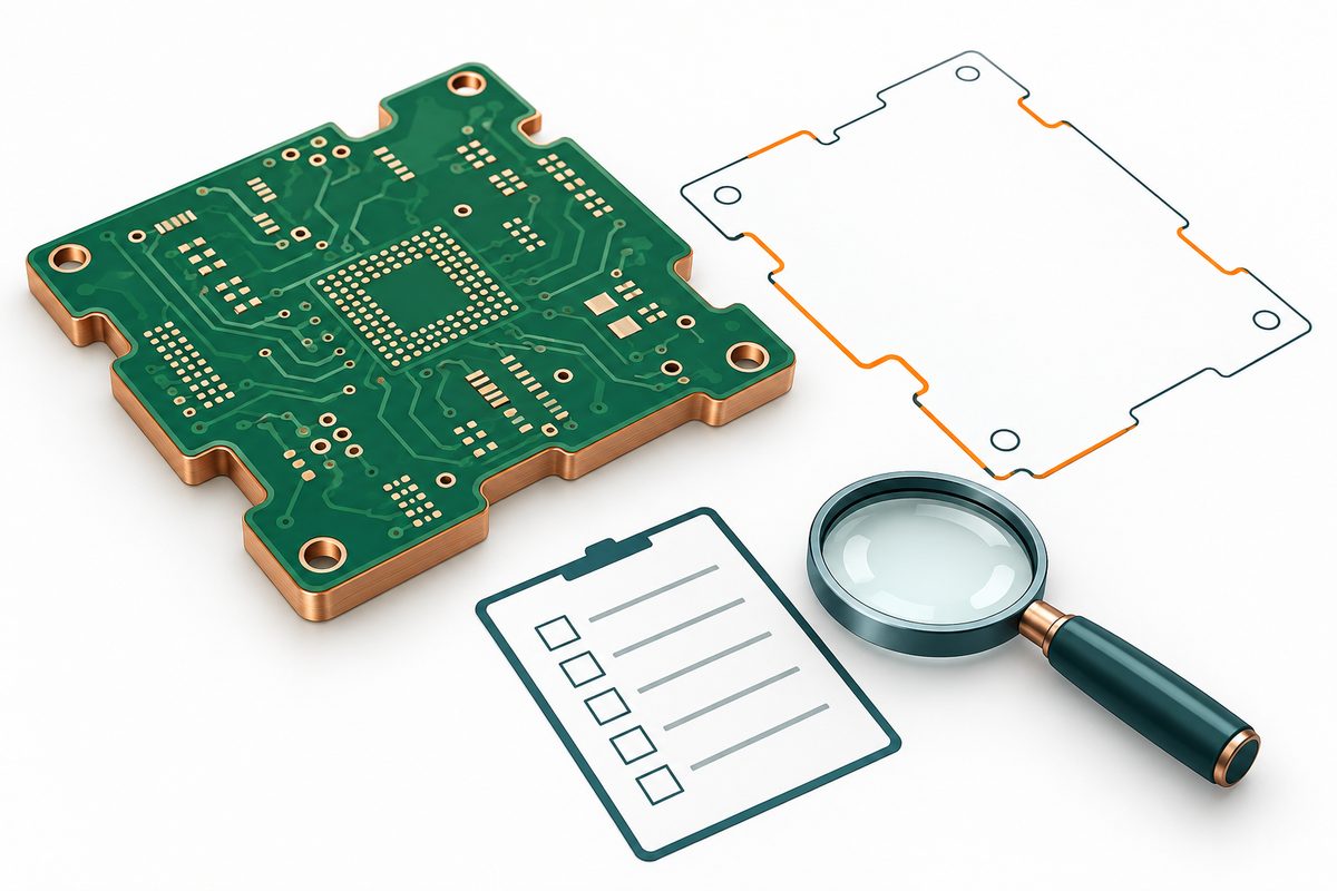
Compare suppliers against the same controlled contour and finish specification. Ask whether panel preparation, special processing, inspection, and requested records are included. A quote that omits a functional edge segment or assumes a different support interruption does not cover the same board.
As a hypothetical example, moving a mounting hole near a plated sidewall may change the available isolation space or panel-support options without changing the board’s overall dimensions. Review the affected copper and contour together. Treat an outline, stackup, finish, or support change as a reason to recheck the interface, not simply reuse the previous purchase note.
Conclusion
PCB edge plating requires a defined electrical interface and a manufacturable contour. Select the connected layers, isolate unrelated copper, agree on support interruptions, and choose the finish for the actual use. Release consistent files and define acceptance evidence before the boards enter production.
Ready to review the design? Submit the manufacturing files, marked plated-edge drawing, stackup, finish and inspection requirements, quantity, and schedule through the online PCB RFQ form for engineering and quotation review. Include the mating-interface requirements so the proposed build can be evaluated against its intended function.
Latest Blog

Contact Info
Phone: +86-755-82882936
Email: [email protected]
WhatsApp: +86-13570802455
Wechat: +86-13570802455
Address: 2nd floor,D Bldg.,Electric Link Technology Bldg.,Gongming,Guangming New Dist.,518106 Shenzhen, China