
6-Layer PCB Stackup Choices That Make Production Easier
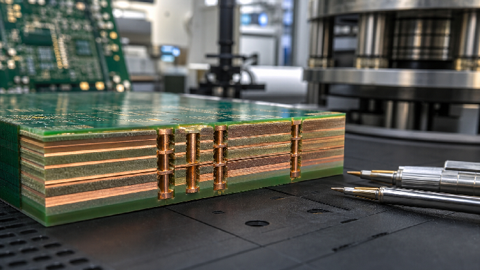
Table of Conent
Table of Conent
A 6-layer PCB is a strong choice when a 4-layer board cannot provide enough routing density, reference planes, or power integrity margin. The extra layers should reduce electrical risk and manufacturing rework, not simply hide messy routing.
Most 6-layer designs serve high-speed digital, mixed-signal, industrial control, RF support circuits, or compact products with dense connectors. The key is stackup discipline. If signal layers do not have nearby reference planes, the layer count is being wasted.
Why Designers Move to 6 Layers
A 6-layer PCB gives you more routing freedom and better plane planning than 4 layers. It also makes it easier to separate noisy, sensitive, and power-heavy areas.
| Design Need | Why 6 Layers Help |
|---|---|
| Dense BGA or connector escape | More routing channels and via strategy options |
| High-speed digital buses | Better reference-plane control |
| Mixed analog and digital | Cleaner partitioning and ground planning |
| Multiple power rails | More controlled power distribution |
| EMC improvement | Smaller current loops and more shielding options |
If the design includes RF or very fast edges, compare stackup planning with our RF PCB and high-frequency PCB guide.
The Design Pattern Behind Many 6-Layer Boards
A common 6-layer candidate is a board that has one main processor or MCU, a switching power stage, a communication interface, and several connectors. On 4 layers, the routing may fit, but the layout starts making compromises: power islands cut through return paths, differential pairs take longer routes, and test pads disappear.
Six layers give the designer room to keep ground intact while routing signals through internal layers. That does not automatically solve every problem, but it gives the design more electrical and manufacturing margin.
The move is especially useful when the board needs to pass EMC testing. A solid reference structure is easier to defend than a layout full of stitched-together ground fragments.
Common 6-Layer PCB Stackups
There is no universal 6-layer stackup, but some arrangements are more practical than others.
| Stackup | Best For | Watch-Out |
|---|---|---|
| Signal / Ground / Signal / Signal / Power / Signal | Routing density | Internal signal layers may couple if spacing is poor |
| Signal / Ground / Signal / Power / Ground / Signal | General high-speed designs | Good balance of routing and reference planes |
| Signal / Ground / Power / Ground / Signal / Signal | Strong plane coupling | Bottom signal layer needs return-path review |
For many products, signal, ground, signal, power, ground, signal is a reliable starting point. It gives outer layers reference planes and keeps power near ground for decoupling.
Stackup Selection by Product Type
| Product Type | Preferred Stackup Direction | Reason |
|---|---|---|
| Industrial controller | Signal / Ground / Signal / Power / Ground / Signal | Balanced routing and EMI control |
| Communication module | Signal / Ground / Signal / Signal / Ground / Signal | More signal routing near ground |
| Power control board | Signal / Ground / Power / Power / Ground / Signal | Better rail distribution |
| Mixed-signal board | Signal / Ground / Signal / Power / Ground / Signal | Separates sensitive and noisy areas |
| Compact processor board | Depends on BGA fanout | Routing density may drive structure |
The stackup should be selected before dense routing begins. If you wait until after layout, the manufacturer may need to force the board into a build that does not match your signal assumptions.
Manufacturing Constraints to Confirm Early
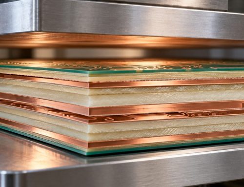
The fabricator must confirm the stackup before production. Six layers require controlled lamination, predictable dielectric spacing, and registration between layers.
Important checks include:
- Finished thickness and tolerance.
- Core and prepreg material selection.
- Copper weight on inner and outer layers.
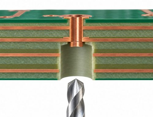
- Minimum mechanical drill and annular ring.
- Via aspect ratio.
- Controlled impedance trace geometry.
- Copper balance and panel layout.
For drill planning, see standard PCB hole drill sizes. For production efficiency, review PCB panelization.
Via Strategy on a 6-Layer PCB
Most 6-layer PCBs can be built with standard plated through vias. That is usually the most economical and robust choice. However, the via size still affects routing density, aspect ratio, and plating reliability.
| Via Approach | Best Use | Manufacturing Note |
|---|---|---|
| Standard through via | General routing | Lowest complexity |
| Small mechanical via | Denser routing | Watch aspect ratio and annular ring |
| Via tenting | Prevent solder wicking | Confirm mask capability |
| Via-in-pad | Special dense packages | Adds filling and plating steps |
| Blind microvia | Usually HDI designs | Not typical unless density requires it |
For many 6-layer boards, the smartest cost decision is not to use advanced vias. Use comfortable through vias, then reserve tighter features for areas that truly need them.
Routing Strategy for a 6-Layer PCB
A clean 6-layer PCB usually follows a simple rule: critical signals need an uninterrupted reference plane. Avoid routing fast nets across plane splits, large voids, or gaps between power islands.
Use these practices:
- 1. Put fast signals on layers adjacent to ground.
- 2. Route differential pairs with consistent spacing.
- 3. Keep decoupling capacitors close to power pins.
- 4. Stitch ground near layer transitions.
- 5. Avoid unnecessary via stubs on very fast nets.
- 6. Keep analog return paths away from switching currents.
A practical example: a motor controller with Ethernet, ADC sensing, and gate drivers may fit on 4 layers, but the ground return and power routing can become fragile. A 6-layer PCB lets the designer dedicate planes and isolate sensitive measurement paths from switching noise.
Power Integrity Planning
Power integrity is not only about wider traces. It is about current loops, decoupling placement, plane spacing, and transient current paths. A 6-layer PCB gives you more options, but the board still needs deliberate planning.
Use short connections from decoupling capacitors to power and ground. Keep high-current switching loops compact. Avoid forcing sensitive analog rails to share noisy return paths. If a rail supplies a fast digital device, make sure the decoupling network has a low-inductance path to the reference plane.
| Power Issue | Layout Fix |
|---|---|
| Voltage dip during switching | Better decoupling placement and plane connection |
| Regulator noise coupling | Short hot loop and local ground control |
| Analog measurement noise | Separate routing and controlled return path |
| Heat concentration | Copper spreading and thermal via planning |
These details are easier to solve before placement is locked.
Cost and Yield Trade-Offs
A 6-layer PCB costs more than 4 layers, but it can reduce total project cost if it prevents EMC failures, layout respins, or assembly complications.
| Decision | Lower Risk | Higher Risk |
|---|---|---|
| Stackup | Confirmed before routing release | Assumed from generic template |
| Via design | Comfortable annular ring | Minimum pad and drill everywhere |
| Copper balance | Symmetric plane planning | Large copper imbalance |
| Test plan | Electrical test plus PCBA inspection | Bare visual inspection only |
| Assembly | BOM and placement reviewed together | Fabrication and assembly separated |
For general multilayer planning, use our multilayer PCB production guide.
DFM Checklist for 6-Layer PCB Release
Before releasing the files, check the design from the fabricator’s point of view.
- 1. Are all drill sizes realistic for the finished board thickness?
- 2. Are annular rings large enough after registration tolerance?
- 3. Are copper pours balanced across the stackup?
- 4. Are high-speed traces routed over continuous reference planes?
- 5. Are plane splits kept away from critical nets?
- 6. Are controlled impedance targets documented?
- 7. Is the surface finish matched to component pitch?
- 8. Are panel rails and tooling holes defined?
- 9. Are test points available for production?
- 10. Are assembly drawings clear enough for polarity and orientation?
This checklist is not paperwork. It is the difference between a board that is simply manufacturable and a board that is easy to manufacture repeatedly.
Testing Plan for 6-Layer Boards
Bare-board electrical test checks continuity, but it does not prove the assembled product works. For complex 6-layer PCBs, plan inspection around the actual component mix.
AOI is useful for visible SMT joints. X-ray helps with hidden terminations. ICT can check nets and component values when test access is designed in. Functional testing confirms the board behaves as intended.
Read more in our PCBA testing process guide.
Frequently Asked Questions About 6-Layer PCBs
Is a 6-layer PCB always better than a 4-layer PCB?
No. A 6-layer board is better only when the added layers solve routing, EMI, power, or density problems. A simple board may not benefit enough to justify the cost.
What thickness is common for 6-layer PCBs?
Many 6-layer boards are still built around 1.6 mm finished thickness, but thickness depends on stackup, impedance, connector requirements, and mechanical constraints.
Do 6-layer PCBs require blind vias?
Usually no. Most 6-layer boards can use through vias. Blind or microvias are considered when package pitch or routing density makes through vias impractical.
Can I use 6 layers for controlled impedance?
Yes. Controlled impedance is common on 6-layer boards, but the manufacturer must confirm dielectric spacing, copper thickness, and trace geometry.
What should I ask my fabricator before routing?
Ask for standard stackup options, material availability, copper weight, drill limits, impedance guidance, and whether your preferred finish supports the assembly plan.
Final Engineering Notes
The strongest 6-layer PCB designs usually look simple after they are finished. Critical nets have clear references. Power rails have planned paths. Vias are not pushed to the process limit everywhere. Test access is still available.
That simplicity comes from early decisions. Confirm the stackup before routing, involve the manufacturer before release, and treat assembly inspection as part of the design. A 6-layer board gives you enough structure to build reliable products, but only if the layers are used with intent.
When 6 Layers Are Not Enough
A 6-layer PCB may not be enough if the design has large BGAs, multiple high-speed interfaces, many power domains, or strict impedance and EMI requirements. In those cases, 8 layers or more can simplify routing and improve reference-plane planning.
Do not choose 6 layers just because it feels cheaper. Choose it when the stackup supports the electrical requirements with enough manufacturability margin.
Bottom Line
A 6-layer PCB works best when the layer plan is intentional: signals near reference planes, power close to ground, vias within process limits, and inspection planned before assembly. AssyPCB can review your stackup, check manufacturability, fabricate the boards, source components, assemble the PCBA, and test the finished product.
Latest Blog

Contact Info
Phone: +86-755-82882936
Email: [email protected]
WhatsApp: +86-13570802455
Wechat: +86-13570802455
Address: 2nd floor,D Bldg.,Electric Link Technology Bldg.,Gongming,Guangming New Dist.,518106 Shenzhen, China