
8-Layer PCB Design Guide for Dense, High-Speed Products
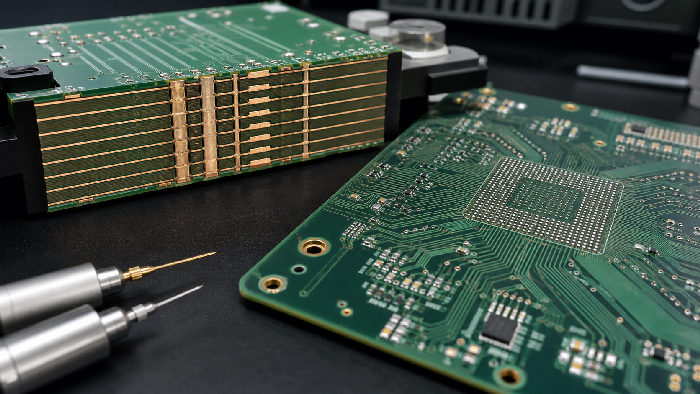
Table of Conent
Table of Conent
An 8-layer PCB is used when routing density, impedance control, EMI performance, or power distribution need more structure than a 6-layer board can provide. The value comes from assigning layers deliberately, especially around reference planes and BGA escape routing.
Eight layers are common in industrial controls, communication modules, embedded computing, medical electronics, and compact products with several power rails. They can be built reliably, but only if the stackup is confirmed before layout release.
Why Use an 8-Layer PCB
The main reason is control. More layers let you place signal layers next to reference planes, separate power domains, and route dense components without cutting up ground.
| Need | 8-Layer Advantage |
|---|---|
| Dense BGA fanout | More escape channels and via options |
| High-speed interfaces | Better impedance and return-path control |
| EMI reduction | More plane shielding and smaller loops |
| Multiple power rails | Cleaner distribution and decoupling |
| Compact enclosure | High routing density in less board area |
For related layer-count planning, see our multilayer PCB guide.
When 6 Layers Start to Feel Crowded
An 8-layer PCB often becomes the right choice when a 6-layer layout technically routes but leaves no margin. You may see long escape routes from a BGA, power rails squeezed between signals, or high-speed pairs changing layers too often.
The board may still pass design rule checks. That does not mean it is a good layout. The purpose of moving to 8 layers is to make routing cleaner, return paths more predictable, and assembly test access easier to preserve.
For engineering teams, the cost increase can be cheaper than a redesign after EMC testing or bring-up failures.
Practical 8-Layer Stackup Options
A common stackup is signal, ground, signal, power, ground, signal, ground or power, signal. The exact order depends on impedance targets and power needs.
| Layer | Typical Function | Design Intent |
|---|---|---|
| L1 | Components and critical signals | Short routes and controlled fanout |
| L2 | Ground | Reference for L1 |
| L3 | Signal | Internal controlled routing |
| L4 | Power | Power distribution |
| L5 | Ground | Plane coupling and shielding |
| L6 | Signal | Internal routing |
| L7 | Power or ground | Depends on rail complexity |
| L8 | Components and slower signals | Secondary routing |
The safest approach is to ask your manufacturer for stackup options before final routing. Dielectric spacing and copper thickness decide whether your trace widths are buildable.
Stackup Goals by Layer Pair
Think in layer pairs, not isolated layers. L1 needs a reference. L3 needs a reference. Internal signal layers should not be sandwiched between noisy or split planes without a plan.
| Goal | Stackup Practice |
|---|---|
| Better EMI control | Put fast signals near solid ground planes |
| Cleaner power delivery | Place power and ground planes close enough for decoupling |
| Easier BGA escape | Reserve internal signal layers for fanout and routing |
| Better manufacturability | Keep copper balanced across the stack |
| Easier debugging | Preserve test points and clear net access |
If a stackup gives every signal layer a clean return path, it is usually easier to tune than one that only maximizes routing layers.
BGA and Via Strategy
Many 8-layer PCBs are driven by BGA routing. The package pitch determines whether you can use through vias, via-in-pad, laser microvias, or an HDI stack.
| BGA Situation | Likely Routing Approach |
|---|---|
| Larger pitch, moderate pin count | Through vias and dog-bone fanout |
| Fine pitch, dense pin field | Via-in-pad or microvias may be needed |
| High-speed memory or processor | Controlled impedance plus reference-plane planning |
| Very compact board | HDI structure may reduce layer pressure |
If your design uses embedded or compact technologies, our article on embedded components on PCBs gives useful context.
Through Via vs HDI Decision
Do not specify HDI just because the board has 8 layers. HDI is useful when it solves a real routing problem, usually around fine-pitch BGA escape or severe board-size constraints.
| Decision Point | Through Via Is Usually Fine When | HDI May Be Needed When |
|---|---|---|
| BGA pitch | Pitch is relaxed enough for dog-bone fanout | Pitch is too tight for mechanical via escape |
| Board size | More area is available | Outline is fixed and dense |
| Speed | Via stubs are acceptable | Very fast channels need shorter transitions |
| Cost target | Cost pressure is high | Performance or density justifies cost |
| Reliability | Standard process is preferred | Supplier has proven HDI control |
The manufacturer should help you compare these options before the layout is locked.
Manufacturing Risks to Control
Eight layers increase the importance of lamination, registration, drilling, and copper balance. The board is still routine for a qualified multilayer factory, but design margins matter.
Confirm:
- Minimum mechanical drill and laser via capability.
- Finished thickness and aspect ratio.
- Annular ring after registration tolerance.
- Sequential lamination needs, if HDI is used.
- Controlled impedance requirements.
- Surface finish for fine-pitch assembly.
- Electrical test and inspection plan.
For drill planning, review standard PCB hole drill sizes.
Signal Integrity and Return Path Rules
An 8-layer PCB can support high-speed routing well, but only if the layer plan is disciplined. The most common problems are not exotic. They are simple return-path breaks, uncontrolled layer changes, and excessive via transitions.
Use these rules:
- Keep differential pairs together through breakouts and layer changes.
- Add ground stitching vias near critical signal transitions.
- Avoid routing fast nets over split planes.
- Keep clock and switching nodes away from sensitive analog areas.
- Confirm impedance geometry with the fabricator.
- Avoid unnecessary via stubs on very fast nets.
If a critical signal changes layers, think about where its return current changes layers. The answer should not be “somewhere nearby.” It should be supported by ground stitching or a clear plane transition.
Cost Trade-Offs
An 8-layer PCB costs more than a 4-layer or 6-layer board, but it can reduce total program risk. The alternative may be a larger board, compromised routing, repeated EMC testing, or difficult assembly.
| Cost Driver | Design Choice That Helps |
|---|---|
| Layer count | Use 8 layers only when routing and planes justify it |
| HDI | Avoid microvias unless package pitch requires them |
| Material | Use standard FR-4 unless speed, heat, or reliability needs more |
| Finish | Choose ENIG for fine pitch and flatness when needed |
| Testing | Add inspection where hidden joints or dense routing create risk |
Panel design also affects cost. See PCB panelization before production release.
DFM Release Checklist for 8-Layer Designs
Before sending an 8-layer PCB to production, check the design against manufacturing and assembly realities.
- 1. Stackup confirmed by the manufacturer.
- 2. Material and Tg selected for assembly temperature and reliability.
- 3. Controlled impedance table included where required.
- 4. Via sizes and aspect ratios within supplier capability.
- 5. BGA fanout reviewed for annular ring and solder mask.
- 6. Copper balance reviewed across layers.
- 7. Surface finish selected for fine-pitch packages.
- 8. Test points preserved for production.
- 9. Panel rails and fiducials defined.
- 10. AOI and X-ray requirements discussed for assembly.
This checklist is especially important when the design moves from prototype to pilot production.
Assembly and Inspection
An 8-layer PCB often carries components that make inspection important. BGAs, QFNs, fine-pitch connectors, and dense decoupling networks need an assembly plan, not just a bare-board order.
Useful checks include solder paste review, stencil aperture review, AOI, X-ray for hidden joints, and functional testing. Our PCBA testing process guide explains these steps.
Frequently Asked Questions About 8-Layer PCBs
Is an 8-layer PCB only for high-speed designs?
No. High-speed designs are common, but 8 layers are also used for dense routing, multiple power rails, compact products, and EMI control.
Can an 8-layer PCB use standard FR-4?
Yes, many can. Use higher-performance material when frequency, loss, temperature, or reliability requirements justify it.
Do 8-layer boards always need microvias?
No. Many 8-layer boards use through vias. Microvias are used when package pitch, density, or signal performance requires them.
What is the biggest design mistake?
Treating added layers as routing space only. The stackup should protect reference planes, power distribution, and manufacturability.
When should the manufacturer review the design?
Before final routing for stackup and impedance, then again before production release for DFM and assembly.
Example: 8-Layer Board for an Embedded Linux Module
Consider an embedded Linux carrier board with a processor module, Ethernet, USB, power conversion, sensor connectors, and a compact enclosure. The design might begin as a 6-layer PCB, but routing quickly becomes crowded around connectors and high-speed interfaces.
An 8-layer stackup lets the designer keep high-speed signals near solid ground while separating power distribution from dense signal routing. The extra layers also leave room for test pads, which are often removed when the design is squeezed too tightly.
The manufacturing benefit is not only better routing. The board becomes easier to inspect and debug. Power rails can be measured. Programming pads can be reached. Critical connectors have clearer escape routing. Those details matter when the product moves beyond the first prototype.
Procurement and DFM Notes
When buying an 8-layer PCB, send the manufacturer the stackup intent and ask for feedback before fabrication. If the board has BGAs, ask them to review the fanout. If it has controlled impedance, ask them to confirm trace geometry. If it will be assembled, send BOM and placement data with the PCB files.
| If the Design Has | Ask For |
|---|---|
| Fine-pitch BGA | Fanout and via review |
| USB, Ethernet, PCIe, LVDS | Impedance and return-path review |
| RF section | Material and finish review |
| Many power rails | Plane and decoupling review |
| Production volume | Panelization and test access review |
The manufacturer should respond with practical recommendations. Good feedback may change pad size, via structure, copper balancing, panel rails, or surface finish. That is not a delay. That is the point of DFM.
Final Design Advice
Use 8 layers when the extra structure helps the product behave predictably. Do not use the added layers as permission to route without discipline. Keep references clean, vias intentional, and test access visible. The board will be easier to manufacture and easier to support later.
Bottom Line
An 8-layer PCB is the right choice when density and signal quality need more structure than lower layer counts can offer. The board should be designed around reference planes, manufacturable vias, controlled stackup, and realistic assembly inspection.
AssyPCB can review your 8-layer stackup, check manufacturability, fabricate the boards, source components, assemble the PCBAs, and test them before shipment.
Latest Blog

Contact Info
Phone: +86-755-82882936
Email: [email protected]
WhatsApp: +86-13570802455
Wechat: +86-13570802455
Address: 2nd floor,D Bldg.,Electric Link Technology Bldg.,Gongming,Guangming New Dist.,518106 Shenzhen, China