
4-Layer PCB Design Decisions That Affect Cost, EMI, and Yield
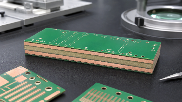
Table of Conent
Table of Conent
A 4-layer PCB is usually the first multilayer choice when a 2-layer board no longer gives you clean routing, stable ground return, or predictable EMI behavior. The extra two layers are most useful when they become reference planes, not just more routing space.
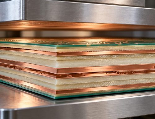
The common stackup is signal, ground, power, signal. It gives outer signal traces a nearby return path, keeps power distribution cleaner, and makes routing easier around dense ICs. For a broader production overview, see our multilayer PCB guide.
When a 4-Layer PCB Makes Sense
Moving from 2 layers to 4 layers adds lamination cost, but it often reduces engineering risk. The decision is usually justified by routing density, noise control, or assembly reliability.
| Design Situation | 2-Layer Risk | 4-Layer Benefit |
|---|---|---|
| MCU with fast edges | Long return loops | Continuous ground plane |
| Mixed analog and digital | Ground cuts and coupling | Cleaner partitioning |
| USB, Ethernet, RF, or clocks | Harder impedance control | Better trace-to-plane geometry |
| Dense connector routing | Many jumpers or vias | More routing freedom |
| EMC-sensitive product | Larger loop area | Lower radiated noise risk |
A practical rule: if the layout needs large ground pours stitched together around many routing cuts, it may already want a 4-layer PCB.
A Realistic Design Trigger
Imagine a compact gateway board with an MCU, Ethernet PHY, DC-DC converter, USB connector, and a few sensor interfaces. On 2 layers, the designer can probably connect everything. The question is whether the return paths are clean enough and whether the board will pass EMC testing without painful rework.
The switch-mode regulator wants short high-current loops. Ethernet wants controlled routing and a quiet reference. The MCU needs decoupling close to power pins. The USB pair should not weave around ground gaps. A 4-layer PCB gives the layout a solid ground plane and a more predictable power structure.
That is the real reason to move to 4 layers. It is not because 4 layers sound more professional. It is because the electrical behavior becomes easier to control.
A Practical 4-Layer Stackup
The best general-purpose 4-layer stackup keeps ground close to the top signal layer. That gives high-speed and noisy nets a short return path.
| Layer | Typical Use | Design Notes |
|---|---|---|
| L1 | Signal and components | Route critical signals here when possible |
| L2 | Solid ground plane | Avoid splits under fast signals |
| L3 | Power plane or power pours | Use local decoupling to L2 |
| L4 | Signal and secondary components | Keep return paths intentional |
Some designs use signal, ground, ground, signal when power is simple and EMI is more important than plane distribution. Others use signal, power, ground, signal. The right answer depends on dielectric spacing, target impedance, and the current path.
Stackup Options Compared
| Stackup | Strength | Weakness |
|---|---|---|
| Signal / Ground / Power / Signal | Good general-purpose balance | L4 return paths need attention |
| Signal / Ground / Ground / Signal | Excellent reference structure | Power must be routed as pours or traces |
| Signal / Power / Ground / Signal | Can work with careful spacing | L1 reference may be less ideal |
| Signal / Signal / Ground / Power | More routing channels | Usually weaker for EMI and high-speed nets |
For most embedded products, start with signal, ground, power, signal. Then adjust based on impedance, power rail complexity, and manufacturer stackup options.
Why Ground Plane Continuity Matters
Fast signals do not return by “finding ground” somewhere on the board. Return current follows the path of least impedance, usually close to the signal trace. If a signal crosses a gap in its reference plane, the return current detours. That detour increases loop area and can increase noise.
This is why a 4-layer PCB with a continuous L2 ground plane can behave much better than a 2-layer board with chopped-up ground pours.
Manufacturing Limits Still Matter
A 4-layer board is not difficult for an experienced fabricator, but it is less forgiving than a 2-layer board. Registration, lamination thickness, drill accuracy, and copper balance all matter.
Pay close attention to:
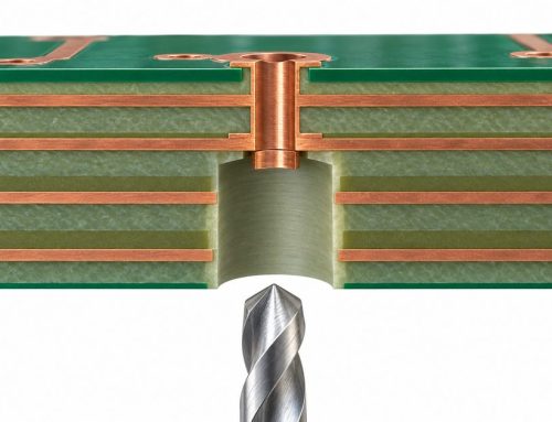
- Minimum mechanical drill size and finished hole tolerance.
- Annular ring after drill wander.
- Via aspect ratio based on final board thickness.
- Copper balance between layers.
- Solder mask clearance on fine-pitch parts.
- Panel rails and tooling holes for assembly.
If you are unsure about drill sizing, review standard PCB hole drill sizes. For panel planning, our PCB panelization guide explains how manufacturability and cost connect.
Controlled Impedance on a 4-Layer PCB
Many 4-layer boards include USB, Ethernet, CAN FD, LVDS, RF control lines, or fast clock nets. Not every one requires formal coupon testing, but the stackup still matters.
Controlled impedance depends on trace width, copper thickness, dielectric constant, dielectric spacing, solder mask, and whether the trace is microstrip or stripline. If you route a 90 ohm USB pair before confirming the stackup, the final impedance may not match the design intent.
| Signal Type | Typical Concern | Design Action |
|---|---|---|
| USB differential pair | Pair impedance and skew | Confirm trace width and spacing |
| Ethernet | Pair routing and reference continuity | Keep pairs over solid ground |
| RF trace | Loss and impedance | Confirm material and finish |
| Clock line | Return path and edge noise | Route near ground and avoid splits |
| Switching regulator node | EMI and loop area | Keep hot loop compact |
Ask the manufacturer to confirm whether their standard 4-layer stackup can meet the geometry you routed. If not, adjust the trace width before fabrication.
4-Layer PCB Cost Drivers
The layer count is only one part of cost. A simple 4-layer board with standard FR-4, 1 oz outer copper, and normal drill sizes can be economical. A compact design with fine traces, dense vias, ENIG, controlled impedance, and fast delivery will cost more.
| Cost Driver | Lower-Cost Direction | Higher-Cost Direction |
|---|---|---|
| Material | Standard FR-4 | High-Tg, low-loss, or special laminate |
| Copper | Standard copper weight | Heavy copper or tight plating requirement |
| Geometry | Comfortable trace and spacing | Fine lines, small vias, tight annular rings |
| Finish | HASL or OSP | ENIG for fine pitch or shelf life |
| Test | Standard electrical test | Controlled impedance coupon and reports |
The cheapest 4-layer PCB is not always the lowest total cost. If a supplier skips stackup confirmation, impedance review, or assembly feedback, savings can disappear during bring-up.
Design Tips That Reduce 4-Layer PCB Rework
The layout stage is where most cost-saving decisions happen. Once the Gerbers are released, every correction becomes slower and more expensive.
Use these practical rules:
- 1. Place the ground plane on L2 unless there is a strong reason not to.
- 2. Keep high-speed traces on layers adjacent to ground.
- 3. Avoid routing signals across plane gaps.
- 4. Stitch ground near connectors and layer changes.
- 5. Keep regulator hot loops small and away from sensitive traces.
- 6. Use enough decoupling, placed close to power pins.
- 7. Confirm board thickness and stackup before impedance routing.
- 8. Leave room for test points on production boards.
Power Plane or Power Pours?
Not every 4-layer PCB needs a full power plane. If the design has one main voltage rail, L3 as a plane works well. If the board has many small rails, L3 may become a set of power islands.
That is acceptable if each rail has a clear return path and decoupling strategy. The mistake is carving L3 into many islands while also expecting it to behave like a clean reference plane.
Assembly Considerations for 4-Layer Boards
A 4-layer PCB often carries finer-pitch components than a 2-layer board. Assembly planning should happen before the board is released.
| Assembly Feature | Check Before Fabrication |
|---|---|
| Fine-pitch ICs | Solder mask clearance and finish flatness |
| QFN packages | Thermal pad design and stencil aperture |
| Connectors | Hole tolerance and mechanical stress |
| Dense passives | Pick-and-place spacing and polarity marks |
| Test pads | Fixture access and probe clearance |
If the same supplier handles fabrication and assembly, ask them to review the BOM and placement data together with the PCB files.
DFM Checks Before Releasing a 4-Layer PCB
Before fabrication, send the manufacturer a complete data package: Gerbers or ODB++, drill files, stackup notes, impedance requirements, board outline, fabrication drawing, and assembly files if PCBA is included.
Ask them to confirm:
- 1. Stackup thickness and dielectric spacing.
- 2. Impedance feasibility for key nets.
- 3. Minimum drill and annular ring compliance.
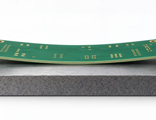
- 4. Copper balance and warpage risk.
- 5. Surface finish suitability for your components.
- 6. Electrical test and inspection plan.
The production sequence is easier to understand if you compare it with how PCB manufacturing works.
Testing and Assembly Planning
A 4-layer PCB often supports more complex electronics, so bare-board testing is only the first checkpoint. Assembly inspection may include automated optical inspection, X-ray for hidden joints, in-circuit testing, or functional testing.
If your board uses BGAs, QFNs, fine-pitch connectors, or power devices, discuss inspection before production. Our PCBA testing process guide explains where AOI, ICT, FCT, and X-ray fit into the workflow.
Frequently Asked Questions About 4-Layer PCBs
Is a 4-layer PCB always better than a 2-layer PCB?
No. A simple low-speed circuit may work perfectly on 2 layers. A 4-layer PCB is better when it solves a real routing, EMI, power, or density problem.
What is the most common 4-layer stackup?
Signal, ground, power, signal is a common starting point. Many engineers prefer it because L2 provides a continuous ground reference for top-layer signals and components.
Can a 4-layer PCB support controlled impedance?
Yes, if the stackup and trace geometry are confirmed. The manufacturer should provide dielectric thickness and copper data before final routing.
Is ENIG required for a 4-layer PCB?
No. ENIG is useful for fine-pitch parts, flat pads, longer storage, or contact surfaces. HASL, lead-free HASL, and OSP can work when the component mix allows.
What should I send to the manufacturer?
Send Gerbers or ODB++, drill files, stackup requirements, fabrication notes, impedance requirements, BOM, placement data, and test instructions if assembly is included.
Bottom Line
A 4-layer PCB is the right move when routing density, EMI, and power integrity need more control than a 2-layer board can provide. The value comes from a disciplined stackup, not just adding copper layers.
Before you order, confirm the stackup, review the return paths, check drilling limits, and make sure the manufacturer understands the assembly plan. AssyPCB can review your 4-layer design, recommend a buildable stackup, and support fabrication through tested assembly.
Latest Blog

Contact Info
Phone: +86-755-82882936
Email: [email protected]
WhatsApp: +86-13570802455
Wechat: +86-13570802455
Address: 2nd floor,D Bldg.,Electric Link Technology Bldg.,Gongming,Guangming New Dist.,518106 Shenzhen, China